There is an entire other dimension to 3D printing, one that more and more companies (Voxel8, Disney, and ChemCubed, among others) are exploring lately: 3D printed electronics and nanotechnology-based conductive inks. Founded in 2012 in Tel Aviv, Nano Dimension is at the forefront of this field and has further increased its lead by receiving a notice of allowance for its Utility Patent Application, related to a unique system for ink recycling and cooling of the printheads.
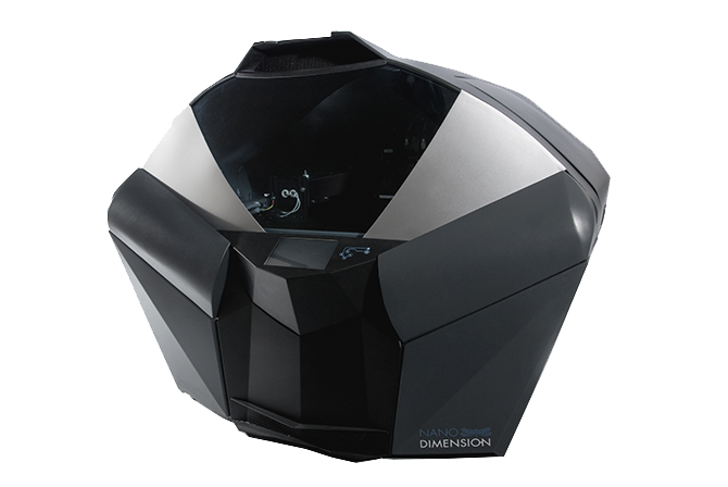
The DragonFly 2020 3D PCB 3D printer, currently in development at Nano Dimension, will thus benefit from this system, developed by the fully-owned subsidiary Nano Dimension Technologies, which will allow unused ink to be conserved, thereby improving the efficiency of the printing process of the 3D printer.
Nano Dimension Technologies applied for this patent in February 2015 and had it approved in less than a year. This is the second time that has happened for the company and Nano Dimension’s CEO, Amit Dror, is clearly enthusiastic about the possibilities that this opens up. “The notice of allowance for our Utility Patent Application acknowledges this technological breakthrough and strengthens both our position in the market as well as our intellectual property portfolio,” he said. “We are glad to receive this notice of allowance after such a short period of time following the filing date.”
Nano Dimension’s novel and proprietary technologies enable the use of conductive ink for ultra-rapid prototyping of complex, high-performance, multilayer printed circuit boards. The company’s DragonFly 2020 3D PCB printer is the result of combining technological breakthroughs in inkjets, 3D printing and nanotechnology. The new patented system is capable of switching between three different modes: inkjet, cleaning, and suction, which allow it to maintain a stable temperature, facilitate cleaning, and make it possible to recycle the ink into the main tank for reuse.
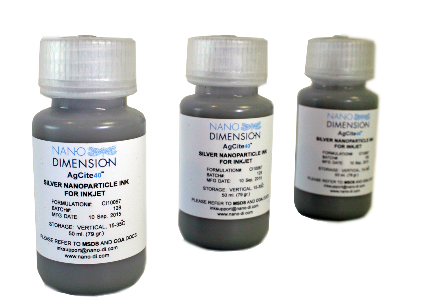
Nano Dimension technology revolves around its “state-of-the-art” AgCite™ line of Nano-particle inks that boast unparalleled conductivity for inkjet deposition (35,700,000 S/m). These integrate 10-100+ nano-meter sized particles of pure silver. And the ability to control the size, shape, and dispersion of the silver nano particles in accordance with printing requirements is critical for formulating the best conductive inks available.
This allows Nano Dimension to achieve the highest ink performance optimization in a wide range of applications including RFID and OLED, from the particle level all the way through formulation to the printing process itself. The AgCite™ family of inks sinters at low temperatures and is suited to a broad range of substrates including paper, polymers, glass and ITO. In the end – even this fascinating 3D printing technology – boils down to the same goal as all other AM: faster prototypes and cost reduction. In the long run, its possibilities are truly endless. Now that the company has received this most recent patent – in addition to raising $12 million in June, being listed on the Tel Aviv Stock Exchange, and planning for a NASDAQ IPO – the possibilities for Nano Dimension seem even more endless.