
Electronics 3D printing is an area of additive still in its infancy. With plenty of space for potential commercial competition, it is interesting to note upcoming developments in the field from the research sphere.
Last month, 3D Printing Industry published an article about a team from the University of Texas at El Paso (UTEP) who demonstrated the potential to 3D print a volumetric circuit, including pre-made components, in virtually any design.
Heralded as a “world first” by the researchers, I wanted to gain some insight into how this development relates to other electronics 3D printers that have already made it to the market.
Speaking with Simon Fried, CBO and co-founder of PCB 3D printing company Nano Dimension, I learn how the UTEP study relates to the technology inside the DragonFly 2020 and 2020 Pro 3D printers.
First, prototyping then, production
As discussed in a previous interview with Fried, electronics 3D printing can be considered as a developing subcategory within the wider additive manufacturing sector. Tipped to follow a similar trajectory as polymers, and now metals, the technology is: first, prototyping then, production.
Though still in the prototyping area of applications, non-planar electronics, i.e. three-dimensional, occupying spaces unconventional to traditional electronics, is the area that 3D printing stands to have real impact. With non-planar ability, and integrated circuits, 3D printed electronics can theoretically be made to fill any space, and form any shape.
As Fried explains, “Printing circuit traces within the body of a part is at the core of what Nano Dimension does.”
CAD for electronics
With the DragonFly 2020 and 2020 Pro systems, it is possible to 3D print PCBs using traditional PCB format files. Such a part is volumetric, “although” Fried adds, “being a PCB it is flat/square/rectangular externally, and the traces are planar internally.”
The overlap between the capabilities of Nano Dimension and the UTEP study however, is the ability to 3D print volumetric circuits using designs that required traditional CAD software. For Nano Dimension volumetric, 3D printable PCB design can be accomplished via a Solidworks add-in launched by the company early 2018.
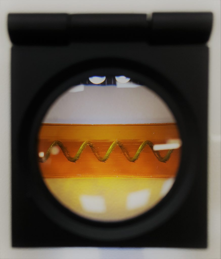
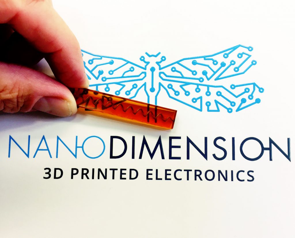
Examples of this volumetric design capability are given by Fried in the form of 3D printed coils and spirals – one integrated into a battery-powdered electromagnet, and another, internally printed conductive trace, which can be seen in the photo below.
Integrated, automated, electronics assembly
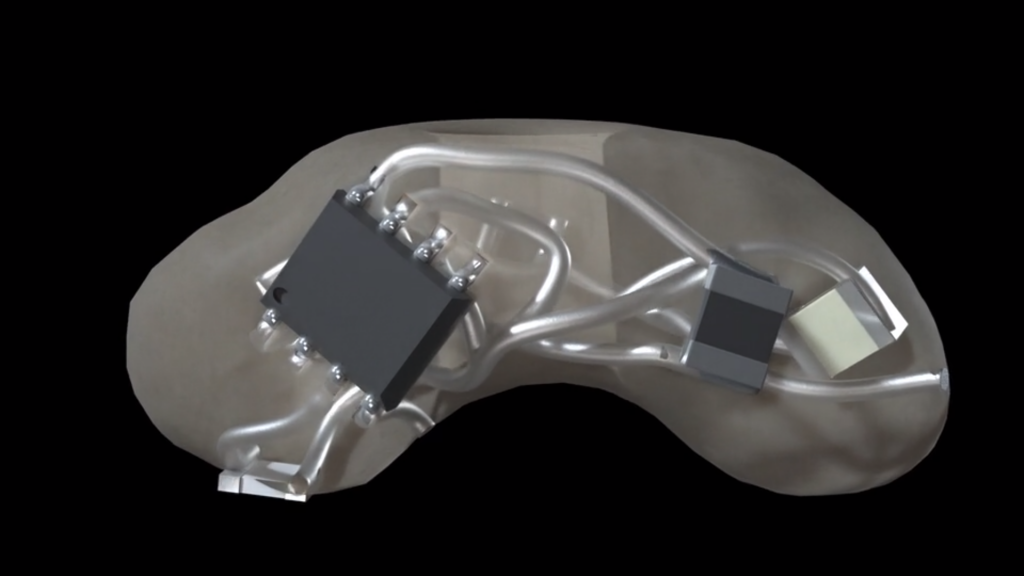
Contrasting Nano Dimension’s 3D printed PCBs, Fried explains, “What is interesting and novel in the UTEP case is the fully 3D outer shape of the part.” Here Fried refers to the jellybean-like shape of the UTEP design circuit (pictured below), which also has a hole in the center.
“We don’t currently use support material so there is a difference in the external geometry/shape that they have produced versus what we print,” adds Fried, “we don’t do external overhangs or undercuts.”
In addition, Fried points to the addition of electrical components on the outer surface of UTEP’s 3D printed part. “This isn’t per-se an innovation as it is already an existing process in the Molded Interconnect Device (MID) industry,” says Fried, “but as an integrated step in 3D printing it is new.” However, this particular development of the UTEP study, Fried notes, is yet to be fully substantiated by the presentation of the team’s 3D printing system and physical parts it has produced, no doubt to be delivered in a published study in the near future.
For more of the latest commentary on electronics 3D printing subscribe to the 3D Printing Industry newsletter, follow us on Twitter and like us on Facebook. Sign up to 3D Printing Jobs to kick start your next career move.
Featured image shows a 3D printed conductive coil encased within a polymer. Photo via Nano Dimension