
In November 2016, Israel’s Nano Dimension (TASE: NNDM) announced that PHYTEC, a leading Embedded Systems Developer, was to be one of the first recipients of a DragonFly 2020 3D printer.
Now a new video demonstrates how 3D printing is integrated within PHYTEC’s product development cycle. Nano Dimension shows how the 3D-printed electronics have helped ramp up prototyping efforts for on demand PCBs.
Saving time and money in a multibillion dollar market
Today printed circuit boards (PCBs) are the backbone of almost every electronic device, from mobile phones and laptops, to industrial control panels and machine interfaces.
To remain competitive within this multibillion dollar industry, electronics manufacturers have to look for new ways to provide fast and high-quality solutions to their customers.
 Gif shows the rapid 3D printing of a circuit board on the DragonFly 2020. Clip via Nano Dimension on Youtube
During the design of a typical electronic device, a PCB at PHYTEC goes through multiple iterations before it is ready for mass production.
As just one part of a larger device, the deadline for a working prototype is usually only a matter of weeks. With traditional manufacturing this first run can take up to 15 days.
Functional PCBs in just one working day
Bodo Huber is the Chief Technology Officer at PHYTEC’s headquarters in Mainz, Germany. By working with Nano Dimension he explains, “The speed of the DragonFly 2020 3D Printer makes it possible for PHYTEC designers to get PCB prototypes 10-15 times faster than the traditional way.”
Expanding on the statement, Huber comments that “It takes us 12-18 hours depending on the size and complexity of a board to print a PCB […] So within one working day, our production facility gets access to the first new PCB of a new design.”
Quality controlled
The rapid turnaround of a DragonFly 2020 3D printed PCB enables PHYTEC to perform functional testing and finalize designs in the early stages of product development.
“Errors can be immediately detected and eliminated”
Once prototyping is complete, the digital file of a DragonFly-realized design is delivered to suppliers in Europe or Asia for mass production. Afterward, the PCBs are delivered to PHYTEC clients around the globe.
Huber adds, “Errors can be immediately detected and eliminated. The result is increased quality of design, faster designs, and shorter design cycles – from months or weeks to days.”
The future of 3D printing
With savings to the product development life cycle, manufacturers can now afford to be more innovative with their designs. Open to customized ink requests, Nano Dimension is working to expand the DragonFly 2020 materials range into ceramic inks and applications in the medical sector.
Simon Fried, Co-Founder and Chief Business Officer of Nano Dimension, gives more insights into the future of 3D printing and how his company are 3D printing electronics.
To stay up to date with the latest 3D printing case studies, sign up to our newsletter, follow us on Twitter and like us on Facebook.
Looking for a new career move or want to recruit in the 3D printing industry? Sign up to our 3D printing jobs site now.
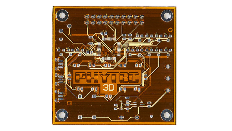
Featured image: Circuit board assembly at PHYTEC. Photo via Nano Dimension