
3D printed electronics are informing the future of our devices. From drones to mobile phones, from laptops to satellites, the technology has the potential to accelerate product development and transform function and design. Non-planar electronics is one area where 3D printing has revolutionary potential.
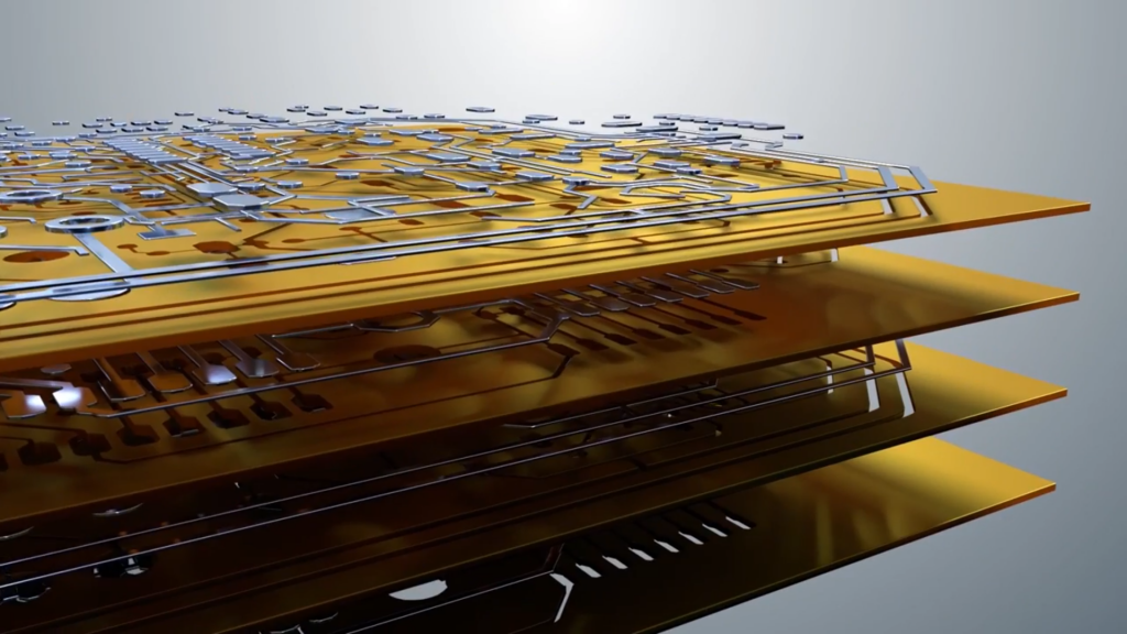
Essentially the antithesis to the traditional stacks of two-dimensional layers in a traditional circuit board, non-planar electronics can enable unique complex shapes, to redefine the limits of traditional electronics.
In this interview Simon Fried, CBO and co-founder of PCB 3D printing company Nano Dimension, discusses the role of 3D printing in non-planar electronics, and the rise of a parallel additive manufacturing sector.
Form follows function
As a multi-hundred billion dollar global market, the electronic sector is faced with the challenge of developing new, lighter and more intuitive devices. This is also a sector where speed of development is crucial. In order to do this, some new tools and some lateral thinking are required.
“Electronics as they’re made today,” explains Fried, “are very planar things.”
“In traditional manufacturing you design in 2D, you manufacture the different layers in 2D, and then you have to complete all kinds of additional process steps like drilling, pressing and plating in order to start connecting those separate layers into a multilayer circuit board.”
“Traditionally everything in a PCB is vertical or horizontal,” adds Fried, noting the synchronicity with 3D printing:
“Layers are crucial in PCB manufacturing and this happens to match additive manufacturing processes very well.”
With 3D printing, designers can turn the traditional process on its head. The manufacturing process and location (in-house) are different, which means development workflows can be more agile at the same time as introducing new design options.
With standard manufacturing methods there are implications to the number of PCB layers you use to make a device. More basic PCBs have 4 layers, others have 6, and more complex devices can contain 16 or more layers. It used to be that large companies had their own traditional PCB manufacturing capabilities but as boards have become so much more complex this is no longer an option.
Prototyping high layer count boards is complex, costly and time consuming. Additive manufacturing changes the way PCBs are manufactured and eases this restriction. Simultaneously 3D printing polymer and metal means PCB interconnects can be built from the bottom up, this makes it possible to prototype complex boards in-house once again. So traditional designs can be printed in-house and novel designs that rely on additive processes can also be evaluated.
“Potentially your signal traces, aka conductive tracers, no longer have to be flat or interconnectedly vertical,” adds Fried “the future will see products where the circuitry is optimally distributed within whatever object you’re printing.”
Using 3D printing to make non-planar electronics
Adding to the advantages of adopting non-planar electronics, Fried continues, “Shaped electronics can allow you to save weight, save space and basically tackle many of the design challenges that today are resolved by resorting to rigi-flex boards which are combinations of traditional, hard PCBs, with lots of flexible ribbons or wires as well as connectors and sockets .”
“[In instances] where the shape of the final product is really important and the electronics have to somehow fit into that shape, you run into challenges such as “how on earth am I going to solve this design and manufacturing challenge, how will it all fit?” Traditional solutions require several manufacturing steps and lots of connectors and parts. If you design for an additive manufacturing approach you can getting rid of connectors and the electronics fit that much better.”
Hailed by some as “the holy grail of 3D printed electronics” one example device given in the course of my conversation with Fried is a cell phone.
“Many of the antennas in smartphones are made by taking a small plastic mold and then adding some conductive tracers to the outside of it. This LDS process is essentially plating onto a shaped piece of plastic” explains Fried.
“This is an application where there is an explicit manufacturing need already – to produce shaped antennas.” With 3D printing, “You could have your circuitry not just on it, you could also have it in it, or a combination of the two.”
“That’s a great shaped electronics application, but antennas is just one area, there are many challenges at the moment in terms of form factor of electrical products, and how exactly you can fit all that functionality into the smaller spaces that today’s products require.”
Cross-industry collaboration
Due to confidentiality agreements, Nano Dimension is not yet at “the case study stage” of its technology, and many specific applications are classified. Indeed, the ability to 3D print PCB’s in-house is highly attractive to companies concerned about maintaining the lead on competitors and wary of leaks.
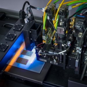
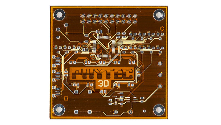
Nano Dimension has a confirmed a partnership with PHYTEC, where the DragonFly 2020 3D printer is in use for prototyping. Advanced manufacturing firms Jabil and FATHOM also own DragonFly 2020 models, alongside undisclosed users in defence, medicine and transportation. In terms of consumer electronics, Fried tells me that wearables, smart watches and electric vehicles are all potential areas of application for this technology.
Speaking of the current and prospective direction of the company, Fried says “I think we’re lucky to be able to play a part in shaping these fundamental changes. I think Nano Dimension and the electronics space are lucky.”
“There is an existing narrative for the adoption of polymer and metal AM in the mechanical space; over the last 10/15 years 3D printing has evolved from a novelty technology to an indispensable driver of innovation in industries that haven’t seen transformational change in decades. This same journey is now underway for the electronics industry.”
Historically, polymer and metal additive manufacturing sectors started as prototyping technologies. Now, both areas are moving to production-scale end-use products and, Fried notes, the developments go hand in hand. For example, as metal gets more popular, polymer responds with stronger, fiber-reinforced materials, and this parallel development is something that is welcomed for the future of 3D printed electronics. “To keep the march of additive manufacturing going, the closer these different technologies work together, the bigger the opportunities are.”
Ultimately, Fried’s vision for Nano Dimension is to simplify the electronics manufacturing process, integrating production and assembly within a single system. “To make a multilayer PCB today you need 40 or even 50 different manufacturing steps, and with a 3D printer you’re looking at a dramatic reduction in manufacturing complexity and the ability to design things differently.” The primary focus at present however is in material development, “As with the mechanical 3D printers, as things evolve into the future what will be required for additive electronics is an ever wider range of materials for broader applications,”
“We are looking to establish complete solutions where it makes sense to do things additively. We expect to be developing materials in order to facilitate printing more varied parts, additional materiales can allow for more flexible electronics, different electrical properties, higher throughputs, higher frequencies,”
“At Nano Dimension we believe that the more value that can be printed into a part, the more compelling the technology becomes. Additive manufacturing of electronics can combine revolutionary electrical functionality with advanced mechanical properties. This can create high value items with a minimum number of process steps.”
To learn more about 3D printing, please visit Nano Dimension.
For more exclusive news and interviews subscribe to the 3D Printing Industry newsletter, find us on Facebook and like us on Twitter. Looking for jobs in engineering? Search open opportunities and apply with 3D Printing Jobs. You can also make a profile to advertise your latest vacancies.
Featured image shows Simon Fried, co-founder and CBO of Nano Dimension. Photo via Nano Dimension