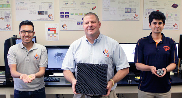
The Electromagnetics and Photonics Lab (EM Lab) of the University of Texas at El Paso (UTEP) has developed an automated process for 3D printing electronics. Incorporating all pre-made components, (e.g. metallic tracks, integrated circuits and transistors) and assembly, the technique enables the fabrication of volumetric circuits with unconventional shapes.
EM Lab research assistant Cesar Valle explains, “Typically, when you make a circuit, it’s two steps. You start with a thin sheet of plastic. On top of that, you form metal traces, then put electrical components onto that,”
“What our tool does that is unique is it combines these processes, and it does it in three dimensions with complete design freedom. We are now able to load 3D files, hit ‘run’ and out comes the part. Literally ‘File,’ ‘Print.'”
Circuits in any form
The EM Lab’s project started with a CAD software developed to design “true” 3D circuits with electric components arranged in any position or orientation. The problem then was a means of physically fabricating the devices. EM Lab doctoral student Gilbert Carranza says, “We couldn’t go anywhere beyond that. We didn’t have the necessary tool to actually translate my design into something that could be read by our 3D printer.”
Valle and Carranza, together with research associate Ubaldo Robles, worked to bridge the gap between CAD and 3D printing capabilities.
In a research paper recently published in IEEE Transactions on Components, Packaging and Manufacturing Technology journal, the team demonstrate the ability to realize circuits as 3D printed tower and bridge structures. These results demonstrate the team’s ability to eventually add 3D printed circuits to an desired form.
Full results of the study, “3-D Printed Structures by Microdispensing Materials Loaded With Dielectric and Magnetic Powders” can be accessed online here.

3D printed electronics
While this development at the EM Lab has been heralded as a “world first” by the team it is worth noting the other industrial and academic names in the 3D printed electronics sector.
Nano Dimension, headquartered in Israel, offers PCB 3D printing in its DragonFly 2020 and 2020 Pro systems. As discussed in an interview with Nano Dimension CBO and co-founder Simon Fried, the area of unconventional, 3D, non-planar electronics holds great potential for the company’s technology.
nScrypt, a provider of micro-dispensing and 3D printing equipment based in Florida, also has a solution for electronics. In a 3D Printing Industry Q&A Ken Church, CEO of nScrypt, said, “The advantages of any shape being electrically functional is obvious, what is less obvious is how to make that a reality. We do not shy away from mature processes that provide improved results, we do however adjust those so they are wholly compatible with 3D printing.”
Dr. Raymond C. Rumpf, director the UTEP EM lab and project lead concludes, “In the future, I don’t think you will see places, such as major electronics manufacturing companies, churning out billions of things and dominating the market nearly as often. Instead, you may have thousands of small businesses in the U.S. churning out thousands of products, both mass-produced and customized,”
“Our 3D circuit technology may be the first step to change the paradigm of circuit manufacturing. And it may enable us to exploit and incorporate new physics in traditional planar (2D) circuitry.”
Stay updated with the latest in additive manufacturing research by subscribing to the 3D Printing Industry newsletter. Also, follow us on Twitter, and like us on Facebook.
Looking for a change of pace or seeking new talent? Search and post 3D Printing Jobs for opportunities and new talent across engineering, marketing, sales and more.
Featured image shows a digital model of the UTEP 3D printed volumetric circuit. Screengrab via UTEP/EM Lab


