
Due to its drop on demand precision, inkjet based 3D printing presents researchers with the stimulating prospect of creating microscopic and complex devices for use in medical and chemical research.
Microfluidics and lab on a chip devices, used to study the effects substances and stimuli, are an emerging method cutting down lab space to conduct complex experiments. Creation of these devices, however, presents researchers with unique challenges, i.e. creating sub-micron channels, and complex internal structures.
At the Swiss Center for Electronics and Microtechnology (CSEM) scientists have developed a method of inkjet printing proving useful for such precise applications.
Two-step inkjet
The CSEM method of inkjet printing operates in between traditional 2D inkjet printing and 3D inkjet printing. It is differentiated from traditional 2D as the structures created are not flat. However, their 3D state is not as complex as other inkjet 3D printed objects. The technology, therefore, is termed 2.5D printing.
The way it works is this. Droplets of ink are deposited in two steps, rather than one.
In the first step, a series of droplets, termed pinning caps, are printed into a desired shape to affix subsequent drops. In the second step, another “layer” of droplets is added. By harnessing the surface tension of the droplets, this second step enables the formation of bridges between initial pinning caps, as demonstrated in the diagram below.
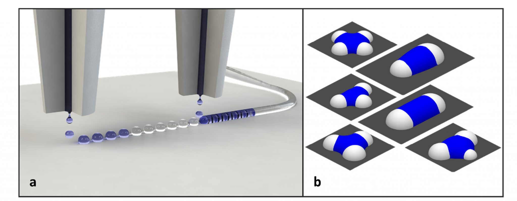
Programming the placement of the caps and the droplets creates straight lines, junctions and corners, that combine to create microscopic channels.
Redirecting light
As a proof of concept, CSEM researchers successfully created optical waveguides using the technique. The picture below shows how an infrared light redirects when shone through a 2.5D printed chip.
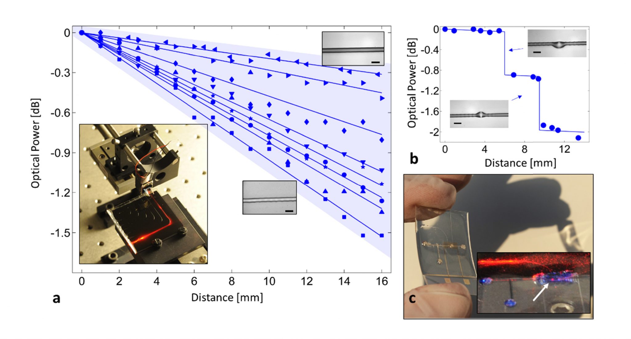
Due to the use of ink, a range of materials can be used in this technique. Metallic inks, for electronic applications, and sucrose mixtures for biodegradable devices, are just two examples that have already been explored by the team.
“The fact that our approach could allow components with multiple functionalities to be fabricated with a single printer paves the way toward additive manufacturing of entire integrated circuits on chips,” explains CSEM researcher Fabian Lütolf.
“This means that optical components could be added to flexible hybrid electronics and that optoelectronic components such as light sources or detectors could be integrated into printed optical circuits.”
“Non-contact printing of optical waveguides using capillary bridges,” is published online in Optics Express journal. It is co-authored by P. M. Theiler, F. Lütolf and R. Ferrini.
For research, materials, business, hardware and software news subscribe to the 3D Printing Industry newsletter, follow us on Twitter, and like us on Facebook.
Search and post 3D Printing Jobs for opportunities and new talent.
Vote for research team of the year and more in the 2018 3D Printing Industry Awards.
Featured image shows two step 2.5D inkjet printing process. Image via Optics Express