
A substantially faster means of producing 3D printed electronics has been devised by a team of researchers from the University of California Los Angeles (UCLA). The new approach is nearly five times quicker than conventional techniques and has the potential to expand the applications of additive manufacturing in consumer electronics such as advanced prosthetics, metamaterials, antennas, and soft robotics.
The UCLA research team’s new two step-method involves lining 3D printed shapes with electrostatic charges, and dipping them repeatedly into a resin mixed with electronically conductive materials. The resin is attracted to the printed shapes, and each dip creates an additional layer on the shape until a 3D structure is formed. This could improve production times by reducing time spent switching between techniques, as is currently necessary with existing multi-process methods.
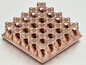
The new 3D printing technique
Many modern mobile phones and laptops contain two-dimensional electronic components such as sensors and antennae, and producing these parts using 3D printing in place of traditional manufacturing methods, has numerous potential benefits. 3D printers are able to produce curves and shapes that aren’t possible by conventional means, which could not only save space inside such devices but also provide the opportunity to improve and develop their internal components.
However, the researchers claim that 3D printed electronics are not widely used because current multiprocess manufacturing methods require print-pausing to change technique. In addition, each individual ink used in the process currently needs to be optimized for the chosen 3D printing technique, requiring significant development time for new materials. This lengthens the overall manufacturing time, and limits the technology’s applications in creating complex 3D electrode interfaces and geometries.
In response, the UCLA’s Samueli School of Engineering has devised its two-step method that significantly reduces the production time needed to produce 3D printed electronics in any preprogrammed 3D shape or design. In the first step, the team used a single optical 3D printer to pattern 3D shapes with pre-programmed electrostatic charges. They then dipped the 3D printed pieces into a solution containing dissolved copper, which is electronically conducting, and the material almost immediately began to organize and stick itself to the designed shapes.
The resulting deposition was clocked at 26,000 mm2h-1, which is nearly five times faster than aerosol jet printing (the next quickest technique), which measured at
5,600 mm2 h-1. This new faster approach allows for parts to be produced with details down to the size of a few tenths of a millimeter. Using electrostatic attraction, the method is able to instantly program conducting materials into any pre-designed 3D feature. It also offers the opportunity to use multiple magnetic materials within the same product, including piezoelectrics and carbon nanotubes.
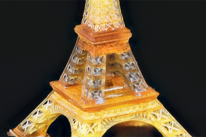
The researchers produced devices such as electronic fingertips and a 2-inch-tall detailed model of the Eiffel Tower with electrodes running throughout its structure, to show how the method can be used to produce electronics with a complex structure. According to assistant professor Xiaoyu Zheng, who led the research team that specializes in combining additive manufacturing techniques with smart materials, the new method could be used to create a range of products containing tactile sensors.
“Our much faster and simpler method can open the door to integrating new classes of 3D electronics, such as lighter, more compact antennas for the next generation of smartphones and 5G communications, or new classes of sensors and smart materials for wearables,” said assistant professor Xiaoyu Zheng.
The researchers’ findings are detailed in their paper titled “Charge-programmed three-dimensional printing for multi-material electronic devices,” which was published in the Nature Electronics journal on April 4th. It is co-authored by Ryan Hensleigh, Huachen Cui, Zhenpeng Xu, Jeffrey Massman, Desheng Yao, John Berrigan, and Xiaoyu Zheng.
3D printing electronics: A background
Although the 3D printing of electronics is still in its relative infancy when compared to other AM applications, new techniques and applications of the technology are constantly being developed. Optomec is one of the early leaders in this sector and uses Aerosol Jet Printing.
Israeli 3D printing electronics company Nano Dimension announced in September 2019 that it was developing 3D printed capacitors using its DragonFly electronics additive manufacturing system. The capacitors are embedded within the company’s 3D printed circuit boards (PCBs), meaning they can both be 3D printed in one job, which saves space and eliminates the need for assembly.
In February 2020, the high-precision micro dispenser manufacturer nScrypt, announced it had successfully 3D printed solder and adhesive dots in the 50-micron range. Using its new SmartPump conical pen tip, the company was able to precisely control the volume of material deposited from its micro dispenser, which is designed for electronics. The method allows solder dots to be printed directly and precisely onto flat and irregularly-shaped electronics boards, which is considered to be a first in 3D produced electronics.
The University of Texas at El Paso (UTEP) has also been developing the 3D printing of electronics, and successfully developed an automated process in 2018. Incorporating all pre-made components and assembly, their technique enabled the fabrication of volumetric circuits with unconventional shapes.
You can now nominate for the 2020 3D Printing Industry Awards. Cast your vote to help decide this year’s winners.
To stay up to date with the latest 3D printing news, don’t forget to subscribe to the 3D Printing Industry newsletter or follow us on Twitter or liking our page on Facebook.
Looking for a job in the additive manufacturing industry? Visit 3D Printing Jobs for a selection of roles in the industry.
Featured image shows a detailed model of the Eiffel Tower produced by UCLA researchers to demonstrate their novel printing technique. Photo via UCLA, Samueli School of Engineering.