
Switzerland-based micro 3D printing company Exaddon has developed the world’s first 3D microprinted probes capable of fine-pitch probing at sub-20 µm pitch. Fine-pitch probe testing is an extremely complex and precise process used to test semiconductor dies.
Optimized for semiconductor wafer testing, Exaddon’s high conductivity probes are 3D printed directly onto customizable and exchangeable space transformers. This reduces complexity, cost, and the number of required component layers.
Exaddon claims that its sub-20 µm capabilities offer significant benefits for the semiconductor industry. Testing at finer pitches enables a greater active die area, which increases yield and reduces chip cost, cutting consumer product costs in the process. Moreover, the company’s template-free micro 3D printing process is highly customizable and capable of fabricating freestanding structures with high aspect ratios.
“The unique capabilities of Exaddon’s μ3D printing technology, made possible by local electrodeposition of pure metal, offers an unprecedented route toward successfully accessing and testing at sub-20 μm pitch,” Exaddion stated in a press release.
“Any application which requires fine pitch probing below the current pitch limit stands to benefit from this unique approach.”
Exaddon 3D microprinting enhances fine-pitch probing
Founded in 2019 as a spin-off from Swiss micro 3D printing company Cytosurge, Exaddon specializes in the additive manufacturing of micro metal parts. Since its launch, the company has established itself as a key provider of 3D printing technology for academic research projects around the world.
The company’s micro 3D printing capabilities, developed over the past two years, seek to meet demand in the $500 billion semiconductor market. Semiconductor manufacturers rely on probe testing of high performance dies to ensure that only Known Good Dies (KDG) make it into their final semiconductor components.
According to Exaddon, probe testing currently struggles to achieve pitches below 40 µm. This is said to limit chip design and restrict the ability of companies to meet consumer demand. For instance, despite the 80% CAGR and multi-billion dollar valuation of the microLED market, LED testing is currently limited to a resource- and time-consuming two-probe approach.
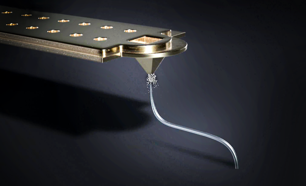
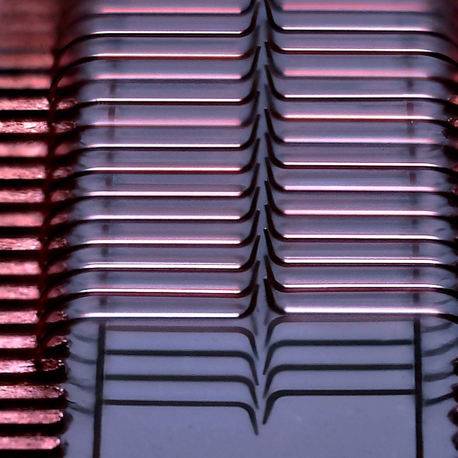
These challenges are overcome by Exaddon’s micro 3D printing technology, which can fabricate high quality metal components measuring less than 20 µm. The Zurich-based company has successfully demonstrated its fine-pitch probe capabilities on µLEDs.
The company’s microLED test array is 3D printed directly on pre-patterned traces with a sub 20 µm pitch. This demonstrator array possesses 128 probes, with a minimum pitch of 18.5 µm in the X-axis, 9.5 µm in the Y-axis, and ±2 μm for the Z-planetary. Exaddon’s probe array, which is around 10% the size of other companies’ probe arrays, reportedly gives microLED testers a 64x increase in efficiency.
What’s more, Exadden’s template-free 3D printing process is highly customizable, and excels at fabricating high aspect ratio, freestanding structures such as coils and lattices. 3D printing directly onto the space transformer simplifies probe card construction, eliminating process steps and components that would otherwise be required. This reduces costs and complexities associated with probe manufacturing.
In the future, the company plans to increase probe count in its μLED arrays and complete WAT (water acceptance test) and CIS (CMOS Image Sensor) probe testing.
Developments in micro 3D printing
Micro 3D printing has been recognized by a number of companies as offering potential within the development and production of electrical devices.
Last year, Austria-based high-precision optical device developer In-Vision announced a collaboration with Professor Tapajyoti Das Gupta of the Indian Institute of Science-Bangalore to develop a new sub-micron 3D printer. Working with Mumbai-based 3D printer manufacturer J Group Robotics, the partners aim to build a 3D printer capable of fabricating nano-scale photonic devices that are flexible and stretchable.
Typically, nano-scale, high-performance optical devices are produced in a multi-step, layered 2D lithography process. This is costly and offers limited scalability, requiring the use of multiple machines in a cleanroom facility.
The team hopes that its new micro 3D printer will accelerate and lower the cost of production, disrupting the semiconductor industry in the process. The first sub-micron optical components are expected to be 3D printed in spring 2024.
Elsewhere, Microfabrication start-up Horizon Microtechnologies offers its own proprietary microscale 3D printing technology. The company’s template-based micro-additive manufacturing (micro-AM) process allows users to produce conductive parts with micrometer-level precision.
This micro 3D printing technology has been designed to offer greater manufacturing versatility in the production of electrodes, electrical contact pins, microfluidic devices, MEMS, and optical packaging.
Subscribe to the 3D Printing Industry newsletter to keep up to date with the latest 3D printing news. You can also follow us on Twitter, like our Facebook page, and subscribe to the 3D Printing Industry Youtube channel to access more exclusive content.
Are you interested in working in the additive manufacturing industry? Visit 3D Printing Jobs to view a selection of available roles and kickstart your career.
Featured image shows a computer render of Exaddon’s template-free 3D print process. Image via Exaddon.