Researchers from the Massachusetts Institute of Technology (MIT) and The University of Texas (UT) at Austin have developed what they claim is the ‘world’s first’ chip-based 3D printer.
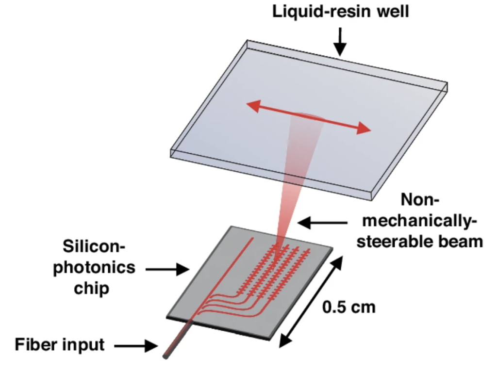
The 3D printer prototype’s coin-sized optical device features no moving parts and is small enough to fit in the palm of a hand. It consists of a millimeter-scale photonic chip that emits reconfigurable light into a vat of liquid photocurable resin.
The resin was designed to rapidly cure when exposed to the visible wavelengths of light emitted by the chip’s array of tiny optical antennas. This allows small structures and patterns to be produced in seconds. The researchers demonstrated the capabilities of the chip-based 3D printer by fabricating a microscale MIT logo, small enough to fit on the face of a US nickel.
According to the team’s research paper, these findings mark the first steps to developing a highly compact, portable and low-cost 3D printer for the fast production of customized parts on the go.
Looking to the future, they hope to develop a small-scale 3D printer with a photonic chip placed at the bottom of a resin well. The chip would emit a 3D hologram of visible light, rapidly curing entire objects via volumetric 3D printing in a single step.
Potential applications of this portable resin 3D printer include customized medical device components and the ability for engineers to quickly fabricate prototypes at job sites.
“This system is completely rethinking what a 3D printer is. It is no longer a big box sitting on a bench in a lab creating objects, but something that is handheld and portable,” stated Jelena Notaros, the study’s senior author and a member of MIT’s Research Laboratory of Electronics. “It is exciting to think about the new applications that could come out of this and how the field of 3D printing could change.”
The first ever chip-based 3D printer
Existing stereolithography (SLA) and digital light processing (DLP) 3D printers are mechanically complex and bulky. This reduces their portability, limiting adoption in applications that require on-site manufacturing. The MIT and UT Austin researchers’ new chip-based approach seeks to address the growing demand for a new compact, portable, and low-cost 3D Printing technology.
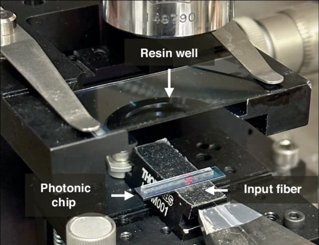
The team’s prototype 3D printer is a single silicon-photonics chip that features an array of 160-nanometer-thick optical antennas. When 3D printing, this was placed below a clear slide containing a small amount of photocurable resin.
To power the chip-based system, an off-chip laser shined a 637-nanometer-wavelength light onto its silicon-nitride waveguide. The antennas then emitted a beam of visible light into the resin.
Successfully modulating visible light is a challenging process, requiring the modification of its amplitude and phase. This can be achieved by heating the chip. However, this method takes up too much space to be compatible with the team’s coin-sized 3D printer.
To overcome this challenge, the researchers produced compact modulators from a liquid-crystal material with unique optical properties. Measuring around 20 microns in length, a set of these modulators were integrated onto the chip.
The crystal molecule modulators were actively tuned using an electrical field to orient them in different directions. This allowed the team to actively control the amplitude and phase of light sent to each antenna.
Once exposed to the external laser beam, the chip’s waveguide distributes a smaller amount of light to each integrated antenna.
Electrical signals were used to non-mechanically steer the light from the antennas, creating shapes that were cured and solidified into physical structures and patterns. Using this approach, the team created a small-scale model of the MIT logo in 6 minutes.
To achieve these results, the researchers also developed a novel photocurable resin compatible with the wavelength of the 3D printer’s natural light source. The UT Austin and MIT teams collaborated to adjust the chemical formulation and concentrations of the liquid resin, creating a formula offering a long shelf life and rapid curing capabilities.
The researchers will now work to develop a volumetric 3D printer that uses holograms of light to fabricate parts in a single step. According to Notaros, this will require them to develop a completely new silicon-photonics chip design, which they hope to showcase in a future research demonstration.
Research enhances resin 3D printing
This is not the first time researchers have sought to enhance the resin 3D printing process. Back in 2019, a team from the University of Michigan developed a high-speed 3D printing process said to be 100 times faster than other commercially available technologies. This technique can fabricate a 3D object with a single flash of light, rather than through the conventional layer-by-layer process.
A vat polymerization technique based on SLA, UMich’s approach is a spin on continuous liquid interface production (CLIP), a method patented by California-based 3D printer provider Carbon. Here, an oxygen-permeable projection window creates a thin polymerization-free area at the bottom of the resin vat. This prevents resin from sticking to the projection window, boosting 3D printing speeds in the process.
In the researcher’s method, a dual light source is used in place of the oxygen membrane used in the CLIP process. Ultraviolet (UV) and blue lights with different wavelengths can be tuned to start or stop the curing process as required. This technique enabled the UMich researchers to achieve 3D printing speeds of approximately 2 m/hour.
Elsewhere, UT Austin researchers collaborated with Lawrence Livermore National Laboratory to investigate the use of metal wire grid polarizing filters in resin 3D printing.
These components are designed to replace the conventional PVA film polarizers used in monochrome LCD screens, which generate patterns for 3D printing individual layers. Testing found that these wired grid polarizers enable a significantly higher light transmission efficiency when compared to their film counterparts.
In liquid-crystal display (LCD) 3D printing, increased transmission efficiency translates to a higher intensity of UV light, shorter 3D printing times, thicker layers, and a wider curing surface.
Want to help select the winners of the 2024 3D Printing Industry Awards? Join the Expert Committee today.
What does the future of 3D printing hold?
What near-term 3D printing trends have been highlighted by industry experts?
Subscribe to the 3D Printing Industry newsletter to keep up to date with the latest 3D printing news.
You can also follow us on Twitter, like our Facebook page, and subscribe to the 3D Printing Industry Youtube channel to access more exclusive content.
Featured image shows a fabricated and packaged photonic chip. Photo via Nature Light Science and Applications.