
Researchers from Lawrence Livermore National Laboratory (LLNL) and The Chinese University of Hong Kong (CUHK) have accelerated the rate of nanoscale additive manufacturing. Tackling what has long been a trade-off between resolution and time, the team have developed a method that could enable industrial-scale production of minute devices. The technique is also capable of creating previously impossible 3D structures with 90-degree overhangs.
Chris Spadaccini, Director of LLNL’s Center for Engineered Materials and Manufacturing, has deemed the research “a breakthrough in nanoscale printing.” In addition, Spadaccini says that the system “will enable the remarkable performance in materials and structures at this size scale to be realized in usable components.”
Further Sourabh Saha, the paper’s lead and corresponding author, explains, “Traditionally, there are tradeoffs between speed and resolution. If you want a faster process, you would lose resolution.”
“We have broken this engineering tradeoff, allowing us to print a thousand times faster with the smallest of features.”
No-compromise nanoscale 3D printing
The method developed by the LLNL/CUHK collective is part of a body of work led by Saha that seeks to improve two-photon lithography. At present two-photon, or multi-photon, lithography is the most common method of 3D printing sub-micron structures. So far, it has been limited however by the speed at which it can 3D print.
In this latest research led by Saha, the solution is to replace the singular laser typically used in two photon lithography systems with a field of light, similar to those used in light projectors. This digital mask controls an ultrafast femtosecond laser, simultaneously projecting one million points into a material vat in a single pass. “This scales up the process dramatically because instead of working with a single point that has to be scanned to create the structure, we can use an entire plane of projected light,” Saha explains.
“Instead of focusing a single point, we have an entire focused plane that can be patterned into arbitrary structures.”
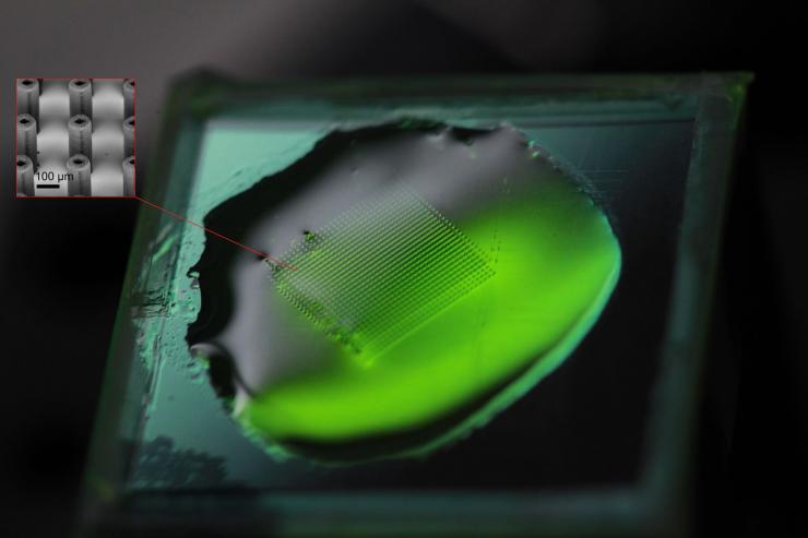
As a demonstration of the method, the team created a series of millimeter-scale structures. In one example, a 2.20 mm × 2.20 mm × 0.25 mm cuboid containing submicrometer lattice features was 3D printed in 8 min 20 s (a rate of 8.7 mm³/hour.) 3D printing the same structure using common two photon lithography would have, by comparison, taken several hours to complete.
Future making of mobile phones
Submicrometer additive manufacturing has a wealth of potential to microelectronics and medical sectors. For Saha at least, “The real application for this would be in industrial-scale production of small devices that may be integrated into larger products, such as components in smartphones.”
Though LLNL and CUHK’s experimentation has so far only worked with polymers the team see potential for the method to be extended across other materials, like metals and ceramics, in the future. The next steps for the team are to continue developing different materials for use in the process, and make improvements to further scale the process.
Saha concludes, “The next questions will be how well we can predict the features and how well we can control the quality over large scales. That will require more work to understand the process itself.”
“Scalable submicrometer additive manufacturing” is published online in Science journal. Credit co-authors are Sourabh K. Saha, Dien Wang, Vu H. Nguyen, Yina Chang, James S. Oakdale and Shih-Chi Chen.
For more cutting-edge 3D printing research subscribe to the 3D Printing Industry newsletter, follow us on Twitter and like us on Facebook. Seeking jobs in engineering? Make your profile on 3D Printing Jobs, or advertise to find experts in your area.
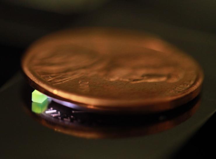
Featured image shows a nanoscale ring structure made using the new high-speed two photon lithography method developed by CUHK and LLNL. Photo via Georgia Tech