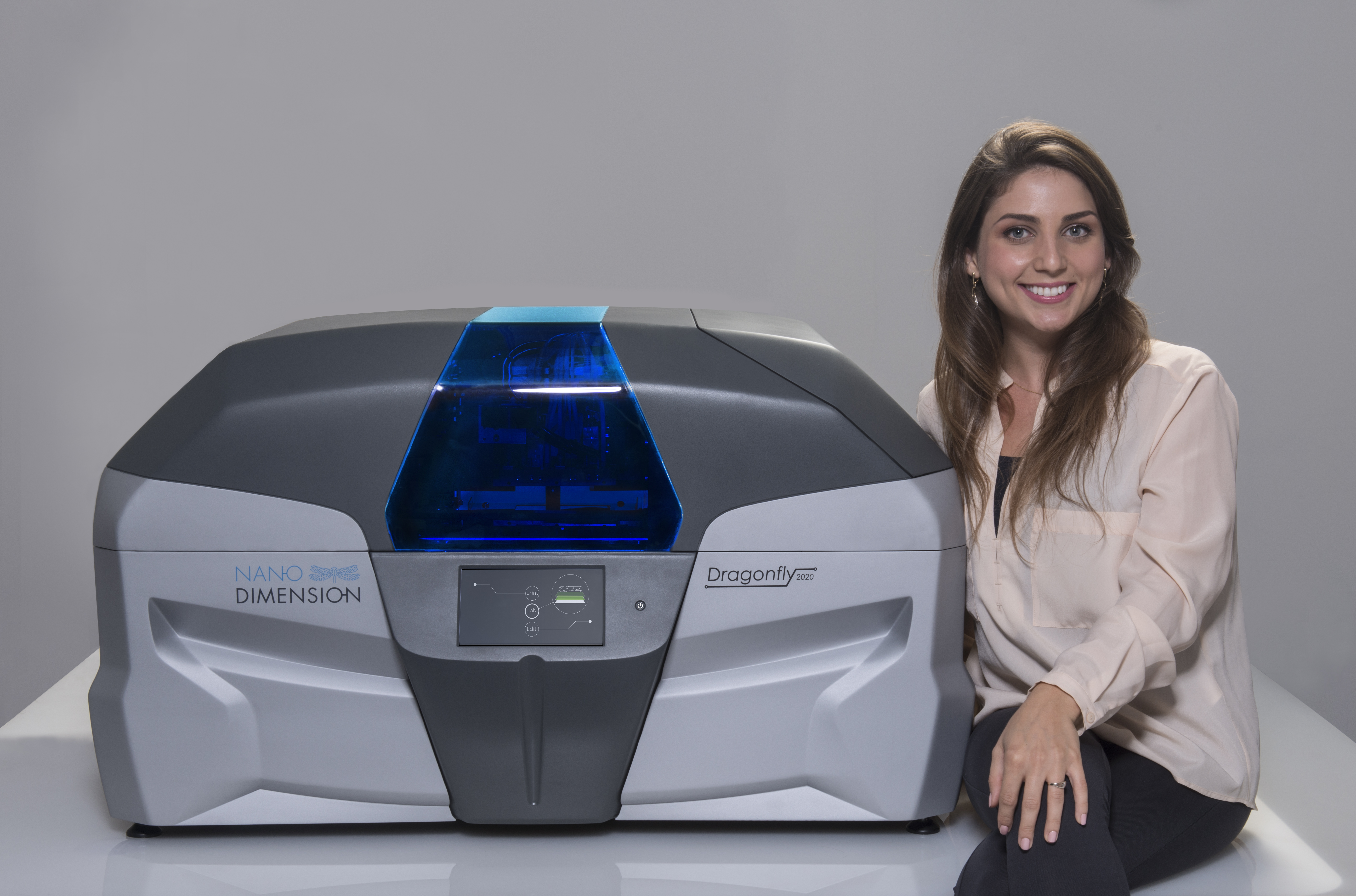
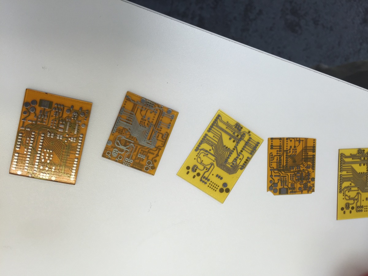
Since being founded in 2012, Israeli electronics 3D printing company Nano Dimension has been a pioneer in the development of conductive and dielectric nano inks and multilayered PCBs (printed circuit boards). In fact, their DragonFly 2020 3D printer is actually the first 3D printer to fully focus on printing circuit boards from nano inks. As recent news seems to indicate, Nano Dimension shows no sign of slowing down their innovation upon the way electronics are manufactured. Coming off of the news that they’d received NASDAQ approval to publicly trade on the stock market, Nano Dimension has now announced a new collaboration with Tel Aviv University to help further develop a nanoparticle nickel material produced by researchers at the university’s labs.
Although nickel is well-known for containing exceptional mechanical properties and high corrosion resistance, the issue with nickel-based nanoparticle ink is its tendency to cluster together, which in turn can cause a clog with the printer nozzle a bit too often. But now, thanks to a unique method developed Professor Gil Markovich and his Tel Aviv University research team, it is now possible to produce nickel nanoparticles that do not cluster together during use in inkjet printing. Using their proprietary technology and well-seasoned knowledge in nano inks and 3D printing electronics, Nano Dimension is aiming to assist Markovich and his team in developing new ink formulations that are specifically tailored for use with their 3D printing technology, particularly through using the nickel nanoparticle ink for applications that include 3D printing sensors with high spatial resolution.
“Implementing this innovative technology with Nano Dimension’s 3D printing process will make it possible to embed sensors within the layers of a PCB,” Nano Dimension said. “A process not possible with conventional manufacturing, opening up a world of possibilities for the monitoring of various energies and their derivatives, such as capacitance, magnetism, temperature and radiation.”
This newly developed nickel nano ink can also be used to protect Nano Dimension’s future PCBs too, as nickel is often used to protect these circuits from oxidation, and therefore the corrosion that follows. This oxidation generally occurs immediately once nano-metric corrosive metals are exposed to air, proving the importance of being able to add protective layers of nickel nano ink during the production process. As the current collaboration between Nano Dimension and Tel Aviv University proves, there is still a lot of groundwork to be done in field of 3D printing functional electronics objects and PCBs. But as Nano Dimension continues to lead the way, it might be time to start looking into buying some shares from their newly formed stock in the NASDAQ market!