While manufacturers have little problem creating large scale metal 3D printed parts, producing metallic objects at a scale to rival the width of a human hair is an altogether more complex process.
By combining ice and electron beam technology, researchers at Zhejiang University, China, are proposing a new method of 3D nanofabrication – and it’s simpler than it sounds (honest).

A new method for making advanced electronics
Electron beam lithography utilizing ice resists (iEBL or Ice EBL) is a development on standard e-beam lithography (EBL), a technique that is commonly used in the low-volume production of small electronic components, like semiconductors.
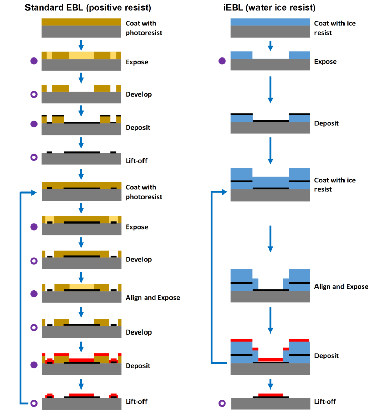
A standard EBL process typically relies on over 10 individual steps for the fabrication of these microdevices. The iEBL process however almost cuts the convoluted steps of standard EBL in half.
By simplifying the technique, this research has the potential to make 3D nanofabrication easier and more accessible to labs, opening doors on innovation for electronics, and other industries, including medicine.
How electron beam lithography works
EBL, in essence, combines moldmaking with 3D printing – instead of building a support material around the 3D object, the support material is laid down first, and determines the shape of each layer.
At the start of a standard EBL process, the base build plate is coated with photoresist material. Selected parts of the photoresist are then exposed to light, causing them to dissolve and leave a pattern for the first layer of an object.
To build these layers up into a 3D object, the photoresist layer must be removed and refreshed each time, making any adjustments needed for the changing shape of the object, i.e. when 3D printing a pyramid in this way, each new photoresist layer should be smaller than the last.

Add a little ice
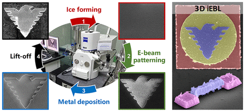
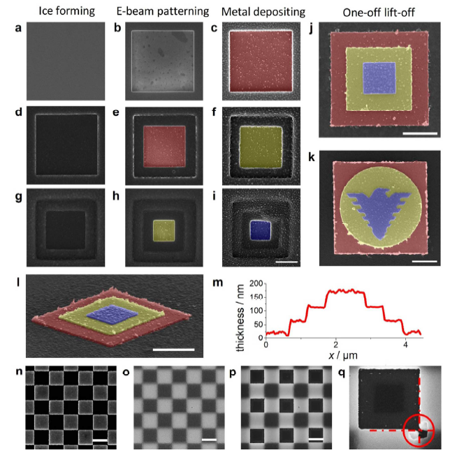
In Zhejiang University’s iEBL method, ice water is used in place of the photoresist material, i.e. each layer of metal film is preceded by a layer of ice, and the desired shape/pattern of the layer is cut out of the ice each time using an electron beam.
What the iEBL method does is cut out the time it taken to develop each layer of photoresist material.
In this preliminary investigation, the Zhejiang team succeeded in shaving around 20 minutes off the total time taken to 3D print a nanopyramind using a standard EBL method.
The sky’s the limit
The method also cuts down on time needed to properly align each layer. Futhermore, the advantage of iEBL over other nano 3D printing technologies, such as two-photon lithography, is in the resolution it can achieve.
Samples shown in the study measure just 3 μm × 3 μm, 2 μm × 2 μm and 1 μm × 1 μm. To give an idea of scale, this castle 3D printed on the tip of a pencil measures 230 μm x 250 μm x 360 μm.

According to the authors’ conclusions “Overall, the iEBL technique needs much fewer processing steps and is almost contamination-free compared to conventional EBL techniques for 3D nanofabrication,”
“It shows great potential in the fabrication of complicated 3D nanodevices for almost all applications, and the only boundary left is our imagination.”
Full results of the study, titled “Three-dimensional in situ electron beam lithography using water ice“, are published online in Nano Letters journal. The paper is co-authored by Yu Hong, Ding Zhao, Dongli Liu, Binze Ma, Guangnan Yao, Qiang Li, Anpan Han, and Min Qiu.
For more breaking research subscribe to the most widely read newsletter in the industry here, like 3D Printing Industry on Facebook and follow us on Twitter. Search and apply for new 3D Printing Jobs here.
Featured image shows Zhejiang University’s eagle logo 3D printed using iEBL. Image via Supporting Information, Nano Letters


