
Researchers from the University of Nottingham’s Centre for Additive Manufacturing have made a breakthrough in the study of 3D printing electronic devices with graphene.
The scientists utilized an inkjet-based 3D printing technique to deposit inks containing tiny flakes of graphene in numerous layers, in a promising step towards replacing single-layer graphene as a contact material for 2D metal semiconductors.
“By linking together fundamental concepts in quantum physics with state-of-the-art-engineering, we have shown how complex devices for controlling electricity and light can be made by printing layers of material that are just a few atoms thick but centimeters across,” explained Mark Fromhold, head of the School of Physics and Astronomy at the University of Nottingham and co-author of the paper.
![]() Graphene and 3D printing
Graphene and 3D printing
Often hailed as a “super material”, graphene is an allotrope of carbon boasting mechanical strength exceeding that of steel, high electrical and thermal conductivity, and exhibits extremely lightweight properties. As such, there has been a flurry of interest and activity within the 3D sector in leveraging graphene and its properties. However, much of graphene’s potential comes from deploying the material in its monolayer form, and the scalability and indeed, the feasibility, of utilizing graphene for 3D printing still presents significant challenges.
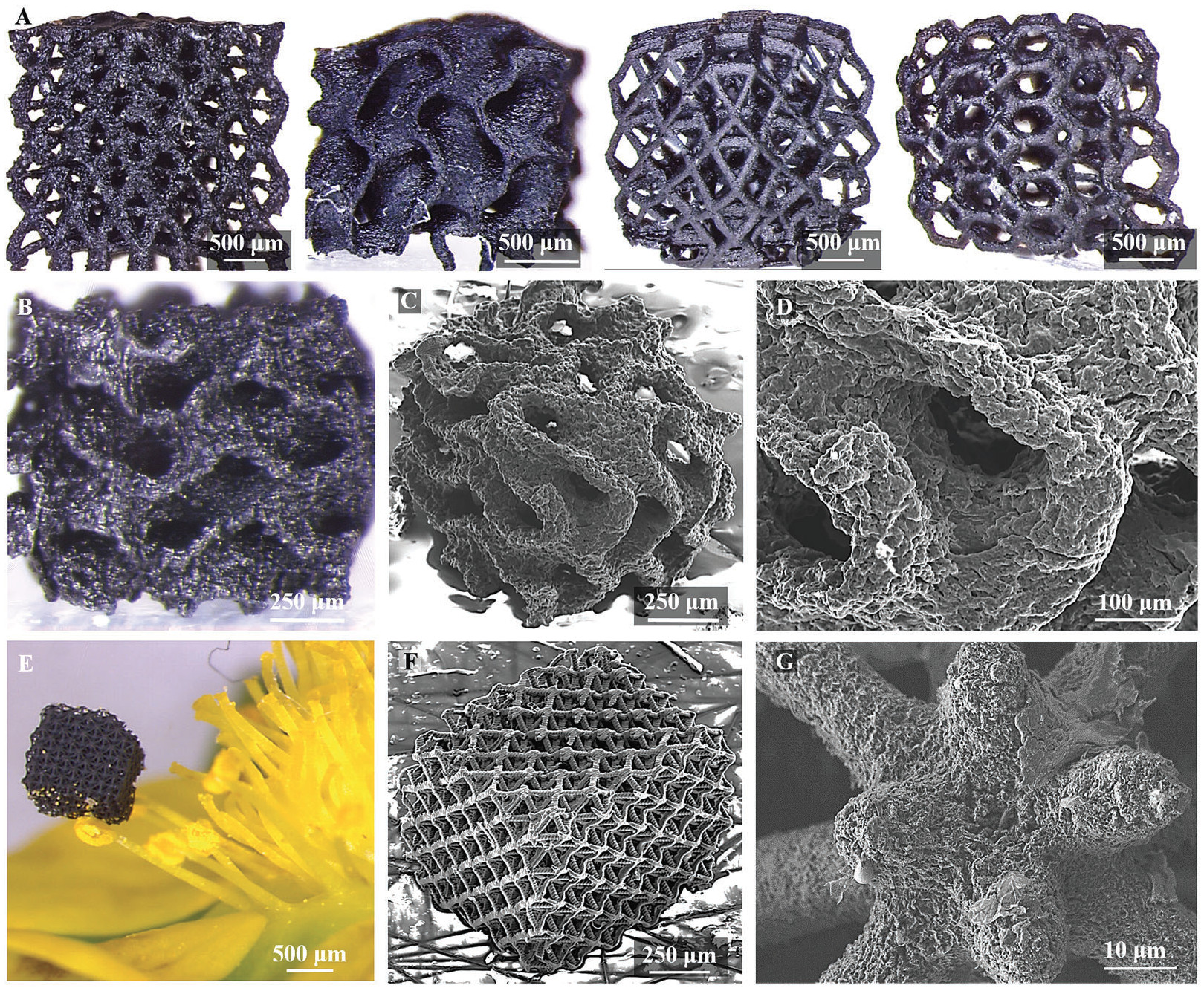
Researchers from Virginia Tech and Lawrence Livermore National Laboratory (LLNL) moved one step closer to harnessing graphene’s true potential after developing a high-resolution method of 3D printing the material, relying on the dispersal of graphene within a gel to make a resin. LLNL also partnered with researchers at the University of California, Santa Cruz, to develop a 3D printing technique for graphene-based aerogel electrodes used within supercapacitors.
Elsewhere, graphene has been used in the fabrication of 3D printed self-sensing armor, and in the modernization of transport networks. Most recently, new research from the Tokyo University of Science revealed how water molecules behave when in contact with the surface of graphene, revealing there is much to learn about the interaction between water and 3D printed materials.
Inkjet printing graphene
Since its discovery, there has been a surge in patents involving graphene, however scalable manufacturing techniques need to be developed in order to fully exploit the material’s potential. This is one of the challenges the CfAM researchers sought to overcome through their research, as they investigated how inkjet-printed graphene could become a potential replacement for single-layer graphene within 2D metal semiconductors.
To do this, the scientists leveraged several advanced manufacturing techniques, including inkjet 3D printing, micro-Raman spectroscopy, thermal gravity analysis, and electrical measurements. Combined, these technologies provided the researchers with a substantial structural and functional understanding of inkjet-printed graphene polymers and the effects of heat treatment on their performance.
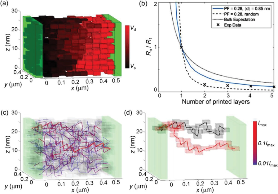
During the study, the researchers 3D printed inks containing tiny flakes of Graphene into multiple layers, to facilitate “inter-flake quantum tunneling”, a process in which the electrical properties of printed layers are strongly influenced by the graphene flakes’ packing fraction, and by meandering electron trajectories which traverse the layers.
“According to the laws of quantum mechanics, in which the electrons act as waves rather than particles, we found electrons in 2D materials travel along complex trajectories between multiple flakes. It appears as if the electrons hop from one flake to another like a frog hopping between overlapping lily pads on the surface of a pond,” explained Fromhold.
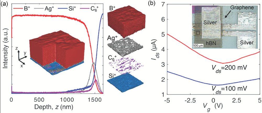
By controlling these trajectories, the scientists were able to produce a fully inkjet‐printed field-effect transistor (FET), consisting of a graphene layer and a top gate of hexagonal boron nitride (hBN). They claim this is the first time that inkjet-printed graphene has successfully replaced single-layer graphene as a contact material for 2D metal chalcogenides – chemical elements also known as the “oxygen family”. The development has thus initiated a new wave of research into 3D printed 2D electronics for photon detectors, sensors, and capacitors, for stretchable and wearable electronics.
“While 2D layers and devices have been 3D printed before, this is the first time anyone has identified how electrons move through them and demonstrated potential uses for the combined printed layers,” said Lyudmila Turyanska of CfAM. “Our results could lead to diverse applications for inkjet-printed graphene-polymer composites and a range of other 2D materials.”
According to Turyanska, in addition to wearable electronics, the findings could aid in the production of a new generation of functional optoelectronic devices, such as large and efficient solar cells and printed computers.
The next steps
Looking ahead, the researchers will explore how to better control the deposition of the graphene flakes within the ink through the use of polymers, and will test several different inks with a range of flake sizes. In this next stage, the scientists will attempt to develop more sophisticated computer simulations of the materials and how they interact, with the ultimate aim to uncover ways of mass-manufacturing the prototype devices.
The study was jointly carried out by CfAM engineers and physicists at the University of Nottingham’s School of Physics and Astronomy under a £5.85 million EPSRC-funded program grant.
The full study can be found in the paper titled “Inter-Flake Quantum Transport of Electrons and Holes in Inkjet-Printed Graphene Devices”, published in the Advanced Functional Materials journal. The paper is co-authored by F. Wang, J. Gosling, G. Trindade, G. Rance, O. Makarovsky, N. Cottam, Z. Kudrynskyi, A. Balanov, M. Greenaway, R. Wildman, R. Hague, C. Tuck, M. Fromhold, and L. Turyanska.
Subscribe to the 3D Printing Industry newsletter for the latest news in additive manufacturing. You can also stay connected by following us on Twitter and liking us on Facebook.
Be sure to subscribe to the Another Dimension podcast on your chosen podcast player to make sure you never miss an episode.
Looking for a career in additive manufacturing? Visit 3D Printing Jobs for a selection of roles in the industry.
Featured image shows representative arrangement of graphene flakes used in the researchers’ Monte Carlo simulation. Image via Advanced Functional Materials.