
A team of researchers at the University of Texas at Dallas Department of Mechanical Engineering have invented an electrochemical-based metal 3D printing method. Named localized pulsed electrodeposition (L-PED), with this method the team has gained in situ control of metal microstructure during the printing process. Free from post-processing too, L-PED enhances the mechanical and electrical properties of 3D printed pure crystalline metals through adjusting the process parameters.
Microscale metal 3D printing with L-PED
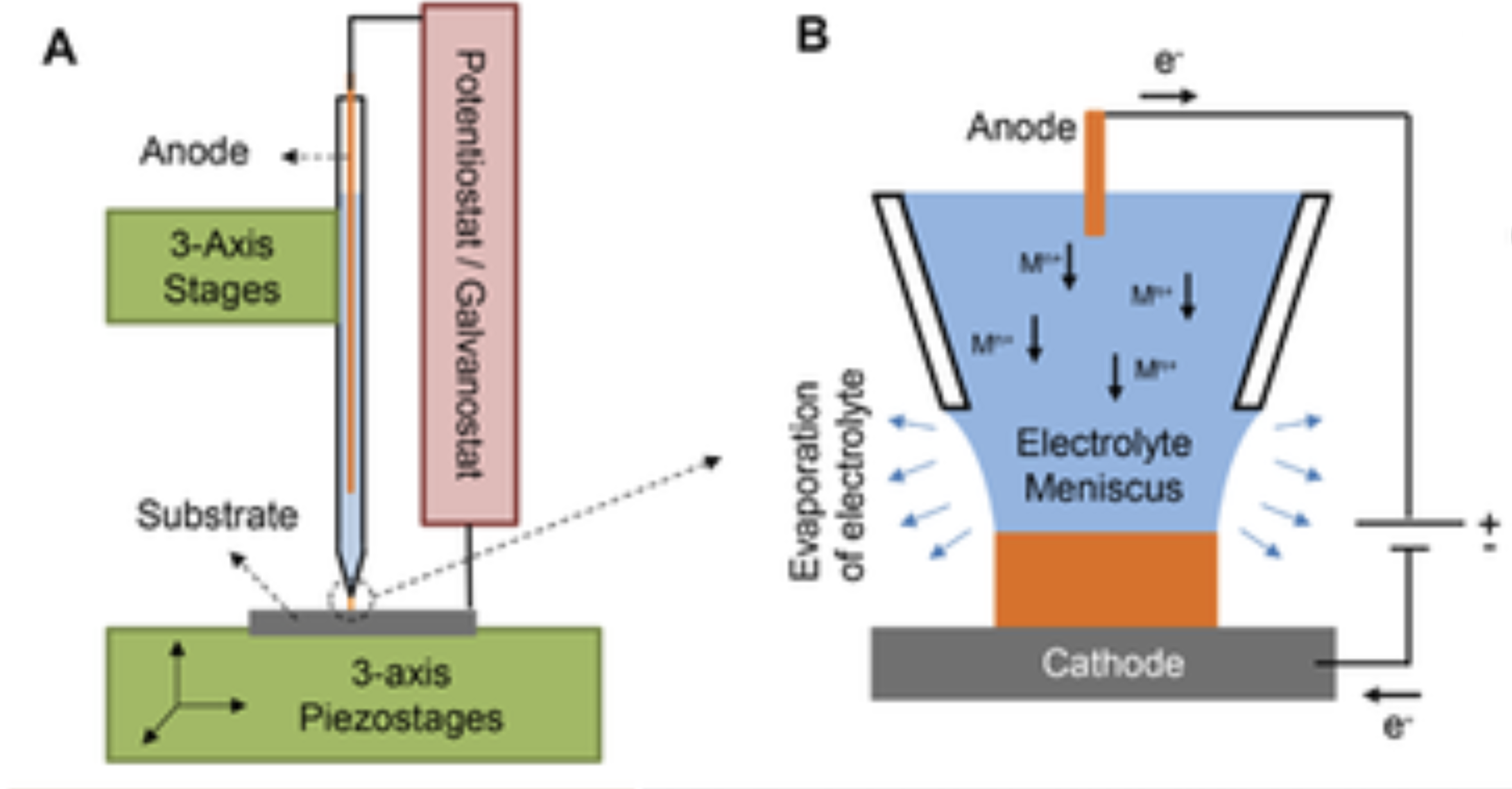
In L-PED, electrodeposition is confined to the nozzle tip with the electrolyte of the chosen metal. When the nozzle approaches the substrate, metal ions are deposited at the meniscus formed between the conductive substrate and the nozzle. A very high current is repeatedly applied between a nozzle and the substrate in intervals of milliseconds.
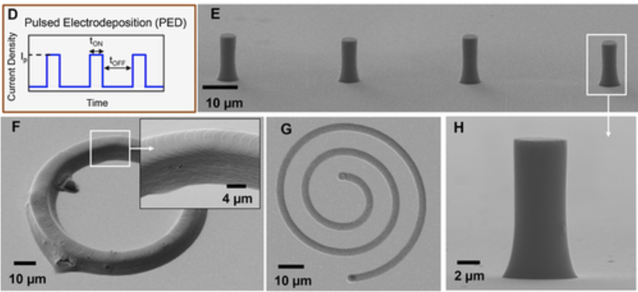
Under standard conditions, the team managed to obtain 90 ± 5% current efficiency, which implies minimal presence of impurities or oxygen. Precise and controlled motion of the relative position of the nozzle and the substrate enable structures to be printed in desired 3D geometries. Different geometries such as free‐standing wires, micro‐pillars (μ‐pillars), and layer‐by‐layer structures can be printed by this method.
Enhancing strength, ductility and electrical conductivity
Using the L-PED process, several tens of copper μ‐pillars were directly 3D printed. Milling from thin films of the material of interest, the focused ion beam fabricated the similar μ‐pillars with average current densities ranging from 2 to 35 nm s^-1. For this range of parameters, all printed copper μ‐pillars contain twin boundaries. The presence of parallel arrays of twin boundaries are known to enhance mechanical and electrical properties.
The critical parameter to control microstructure in L-PED is the average current density. Average current density is directly proportional to the average deposition rate. As deposition rate increases, the density of twin boundaries increases. Randomly oriented grains become more columnar and smaller in size. The twin boundaries within grains become more aligned.
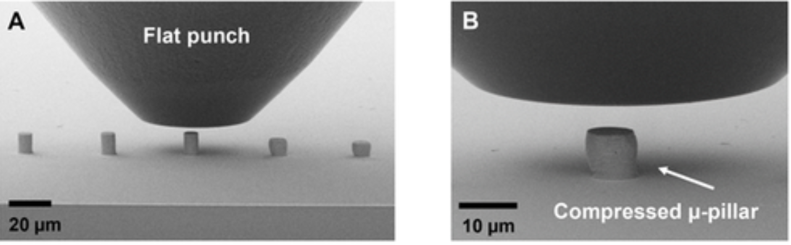
To investigate the microstructure-property relationship of the printed copper, the pillars were then tested in the in situ SEM micro-compression experiment. Results from the in situ SEM nanochemical experiments show ≈1.7‐fold increase in the average current density results in ≈1.4‐fold increase in the deposition rate of the metal, which results in ≈44% enhancement in the flow stress of the printed metal. Specifically, the flow stress of the 3D printed copper can be tuned to 3–5 times of the bulk copper by changing the microstructure during printing.
The researchers have successfully demonstrated control over the density and orientations of the twin boundaries and grain size through controlling the average current density. The fine-grained copper 3D printed with well-aligned and high density of twin boundaries is shown to have high strength, ductility and electrical conductivity.
Microscale metal additive manufacturing
While the current focus of microscale AM is on creating minuscule structures with complex geometries, one of the most formidable challenges facing the industry is control over the material properties of printed metals.
Examples of currently available physical and chemical metal μ‐AM processes are direct ink writing (DIW) and electrohydrodynamic printing (EHD). DIW and EHD often require heat treatment to remove the organic matrix from the printed composite. Often as high as 400–500 °C, pronounced porosity, densification and grain growth of the metallic phase often occur during post-processing.
Achieving in situ control over the microstructure, L-PED is significantly better than the currently available processes for patterning and 3D printing metals. Soheil Daryadel, one of the study’s co-authors states, “This important advancement eliminates the need for post-processing to engineer the microstructure, which often has undesirable consequences for material properties.”
For its attractive material properties, L-PED paves the way for implementing metal μ-AM for functional applications, such as electronic devices, microelectromechanical systems (MEMS), optics, and sensors. Currently, only a limited number of metals including copper, platinum, gold can be deposited. Future work remains to print other metals and alloys through L-PED.
Referencing papers: “Toward Control of Microstructure in Microscale Additive Manufacturing of Copper Using Localized Electrodeposition” is published online in Advanced Engineering Materials journal. It is co-authored by Soheil Daryadel, Ali Behroozfar and Majid Minary‐Jolandan.
Subscribe to the 3D Printing Industry newsletter for the latest additive manufacturing research updates. You can also keep connected by following us on Twitter and liking us on Facebook.
Looking for a career in additive manufacturing? Visit 3D Printing Jobs for a selection of roles in the industry.