
A team of researchers from Oak Ridge National Laboratory and the University of Tennessee have developed a new method of 3D printing electrodes for complementary metal-oxide-semiconductor (CMOS) circuitry.
Specifically, the scientists used a Nanoscribe Photonic Professional GT two-photon polymerization system to nanoprint polymer structures directly onto semiconductor chips, where they can be carbonized. The team believes the method could have major implications for the production of carbon-based biocompatible electrodes, which are an integral part of biosensing devices.
Nickolay Lavrik, co-author of the study, states: “We’ve shown that you can convert a polymer to carbon directly on a chip in a way that can be useful for electrochemical sensing.”
Biocompatible electrodes in neurotechnology
Biocompatible electrodes are often used bidirectionally in neurotechnology, whereby they can record signals from the nervous system as well as deliver stimulation to living tissues. Carbon-based materials, in particular, are great for the application as they can be used to detect glucose, serotonin, dopamine, and other biological molecules. Unfortunately, existing carbon microfabrication techniques are not always compatible with the CMOS chips that power many of today’s advanced electronic medical devices.
The main issue is usually temperature, as electrodes derived from polymers require high processing temperatures of up to 900°C for carbonization to occur (everything apart from the carbon content gets burned away). This can result in the degradation of the surrounding components on the CMOS chip, rendering the device useless.

Carbonizing electrodes on CMOS chips
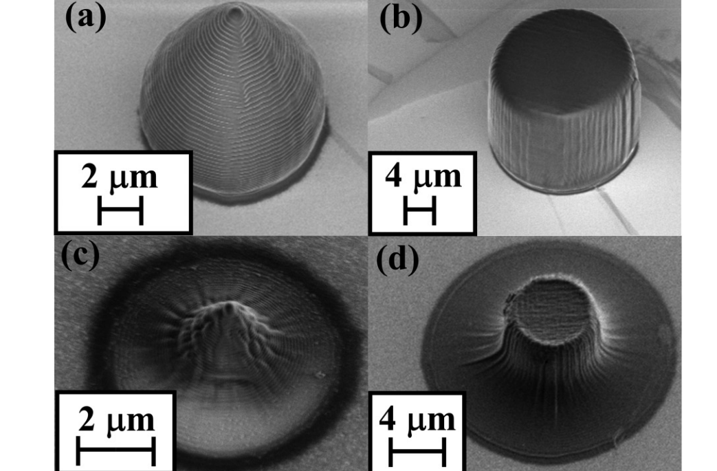
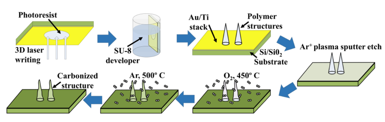
The team started off by nanoprinting two different electrode geometries directly onto bare silicon CMOS chips. The cone-shaped and cylindrical structures were of varying sizes (5 – 20 microns) and fabricated using Nanoscribe’s own liquid photopolymer resin.
Electron beam evaporation was then used to deposit titanium and gold films onto every section of the CMOS chips, except the printed polymer structures. In this case, the titanium served to isolate the electrodes and insulate them from the surrounding components via an oxide layer. The gold, on the other hand, provided reflectivity.
The chips were then annealed in both oxidative and inert environments at 450°C and 500°C respectively, using a high-power laser. With the titanium oxide and gold acting as protective barriers, the exposed polymer electrodes were carbonized in sub-550°C conditions, leaving the other components on the chip completely unscathed and operational. As such, the innovative fabrication sequence yielded highly-customizable CMOS-compatible electrode geometries, showing great potential for electrochemical sensing applications.
Further details of the study can be found in the paper titled ‘Carbonization of 3D printed polymer structures for CMOS-compatible electrochemical sensors’. It is co-authored by Mohammad Aminul Haque, Nickolay V. Lavrik, Ava Hedayatipour, Dale Hensley, Dayrl P. Briggs, and Nicole McFarlane.
3D printed electronics are an area of additive manufacturing that has gained some serious traction in recent years. In fact, Nextflex, a U.S. consortium of companies dedicated to advancing Flexible Hybrid Electronics (FHE), recently entered into a cost-sharing agreement with the Air Force Research Laboratory to advance the sector. Specifically, the deal will see the armed forces shell out up to $154M over the next seven years to fund the development of 3D printed electronics that can support military operations and defense manufacturing.
Earlier this year, military sensor specialist HENSOLDT and 3D printer manufacturer Nano Dimension announced the successful 3D printing of a double-sided ten layer PCB (printed circuit board). The “major breakthrough”, as well as being a world first, is a step toward developing high-performance electronic components through additive means. HENSOLDT is currently in the process of developing the work for military applications such as radar and optronics.
Subscribe to the 3D Printing Industry newsletter for the latest news in additive manufacturing. You can also stay connected by following us on Twitter and liking us on Facebook.
Looking for a career in additive manufacturing? Visit 3D Printing Jobs for a selection of roles in the industry.
Featured image shows the 3D nanoprinted electrode structures. Image via ORNL.