
Oak Ridge National Laboratory (ORNL), Tennessee, is known for 3D printing large objects, such as their airplane part that made it into the Guinness World Book of Records and the 3D printed vehicles they displayed during Chicago’s IMTS.

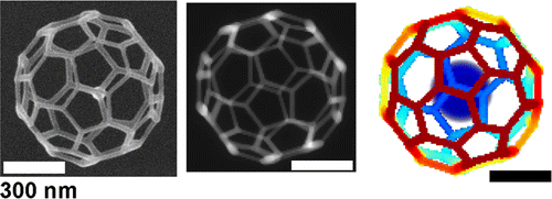
Now ORNL are working at the opposite end of the scale. The lab has 3D printed nanoscale structures that are even smaller than bacteria.
ORNL researchers Philip D. Rack and Jason D. Fowlkes worked with Robert Winkler and Harald Plank of the Graz Centre for Electron Microscopy, Austria, and Brett B. Lewis from The Michael G. Stanford from the University of Tennessee on the project. The full paper of their findings can be found published here, in ACS NANO.
Made by electron beam lasers
The 3D print was done using Focused Electron Beam Induced Deposition (FEBID). Electron beams are used in nanoscale manufacturing for the precise control they offer. In this case an electron beam is used to make a complex, three-dimensional shape, by reacting gas molecules on a controlled surface.
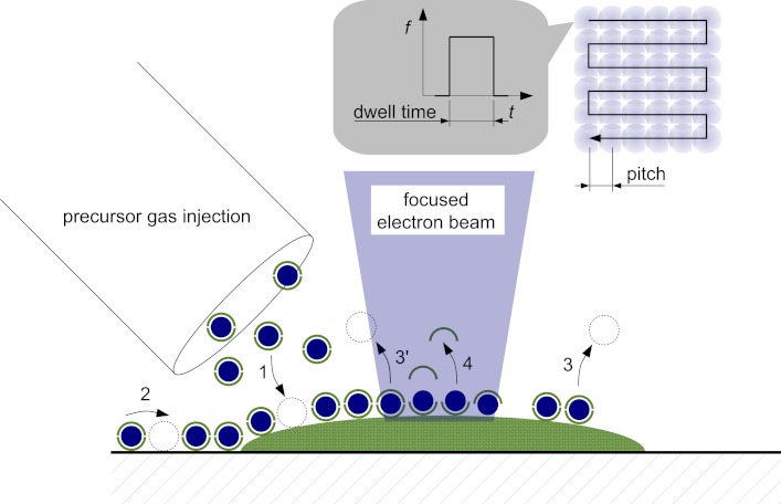
FEBID is a direct-writing method of fabrication that involves computer aided 3D simulation, and 3D design (CAD). Through simulation researchers were able to predict the degrees necessary to move the electron beam in order to create desired geometric shapes.
The above .gif image shows a rotating simulation of the electron beam (represented by the grey arrow and green lines) building up a 3D geometry. Clip via: Oak Ridge National Laboratory on YouTube
Conclusions
After having explained how 2D simulation methods are ultimately inadequate to create 3D structures, successful lattice construction confirmed that 3D simulation is essential to FEBID. The finding also confirm that the speed of the process could be improved in the future through the use of more powerful computers. Calculations for such a small scale are highly complicated and sometimes slow down simulation.
Engineering materials for a better future
Multiphoton lithography is another technique researchers are using to fabricate 3D nanostructures. Using light sensitive materials researchers at TU Wien in Vienna fabricated a castle onto the tip of a pencil.

Nanomanufacturing could develop advanced metamaterials and optoelectronics.
Metamaterials are materials with properties not typically found in nature. For example, a ceramic nanotruss that can return to its original shape after being squashed. Ceramic nanotrusses are used to fuse and fix bone fractures.
Optoelectronics are electronic devices that control light. For example, fiber optic cables for broadband internet. Applying nanomaterials to fiber optic broadband could help give higher-speed internet access – and who doesn’t want that?
Featured image shows a complex nanolattice structure. Image: D. Jang / Caltech.edu