The medical research fraternity is imagining a future where nanoelectronic devicescould detect the concentrations of biomolecules in real time for use as medical diagnostics or interact with single cells for use in basic biological research. Such miniaturization to nanoscale 3D structures and devices would open up possibilities to enable new approaches for health monitoring, surveillance, computer processing, energy research, defense technology and many more applications.
These futuristic nano-devices are being made real by a new technology known as focused electron beam induced deposition (FEBID), a direct beam writing technique for nano and micro structures, which is a nano-scale version of today’s 3D printing processes. Similar to advanced 3D printing enabled additive manufacturing techniques, FEBID aids rapid atom-by-atom “direct writing” of materials with controlled shape and topology. This results in nano-structures down to the sub-100 nm scale, which is highly improbable to achieve with traditional processes.
Although first used in 1976 for demonstrating the nano-patterning capabilities of focused electron beam, FEBID has garnered the interest of researchers only in the last decade, evident from the fact that the number of citations for “FEBID” in academic and scientific journals has increased by a factor of 15 as compared with the 1980’s. The augmented interest in the subject can be attributed to the availability of high-resolution tools, combined with focused ion beam (FIB) processing techniques. Also available is the technology for focused electron beam induced etching, now routinely used in high-end tools for photolithographic (process of transferring geometric shapes) mask repair in the semiconductor industry.
Realizing the impetus of this promising new technology, the Department of Energy grant will fund research to advance an additive manufacturing technique for fabricating 3D nano-scale structures from a variety of materials. The research will focus on dramatically accelerating growth, improving the purity and increasing the aspect ratio of the 3D structures. Researchers expect the three-year $660,000 grant will help them to develop a fundamental understanding of how the process works, accelerate the rate of materials growth and provide improved control over the process. The research will include both theoretical modelling and experimental evaluation.
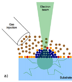
The FEBID technique delivers a tightly-focused beam of high energy electrons and an energetic jet of thermally excited precursor gases – both confined to the same spot on a substrate. Secondary electrons generated when the electron beam strikes the substrate cause decomposition of the precursor molecules, forming nano-scale 3D structures whose size, shape and location can be precisely controlled.
“Wherever electrons strike the surface, you can grow the deposit,” explains Andrei Fedorov, the project’s leader and a professor in the George W. Woodruff School of Mechanical Engineering at the Georgia Institute of Technology. “This provides a tool for growing complex three-dimensional structures from a variety of materials with resolution at the tens of nanometers.”
This process is parallel to the commercially popular “additive manufacturing“ process where a laser-sintering device applies thin layers of the powder material to the building platform followed by a powerful laser beam that fuses the powder at exactly the points defined by the computer-generated component design data. The material is fused so as to bond with the layer below at the predefined points forming components using 3D printing at a macro-scale.
In spite of pioneering advancements, the FEBID process is not free from challenges, namely (i) increasing the rate of deposition, (ii) eliminating the unwanted deposits of carbon that are formed as part of the process, and (iii) availability of micron-scale focused jets to release thermally energized precursor molecules. Through experimentation with inert gasses and playing with new substrate materials, scientists are developing solutions to deal with the hurdles. However, one major limitation to this technology remains — overcoming the scalability barriers to produce nano-devices for mass production, as economies of scales do not play a persuasive role in controlling costs in an additive manufacturing process.
The FEBID process of nano-scale additive manufacturing so far has successfully yielded about two-dozen materials on different substrates, including semiconductors, dielectrics, metals and even plastics. The researchers also plan to create nanostructures containing more than one material, allowing them to craft unique properties not available in each individual material. Examples might include new types of ferromagnetic materials and photonic bandgap structures with unique properties. As Dr. Federov puts it, not uniquely, “the possibilities are almost limitless.”
References:
1. “Grant Funds Development of Improved Nanoscale Additive Manufacturing” http://www.news.gatech.edu/2013/10/21/grant-funds-development-improved-nanoscale-additive-manufacturing
2. “Focused Electron Beam Induced Deposition – Principles and Applications” by Michael Huth, Physikalisches Institut, Goethe-Universita¨t, Germany. www.beilstein-institut.de/Bozen2010/Proceedings/Huth/Huth.pdf