
Researchers at the National Institute of Standards and Technology (NIST) have developed a new method of 3D printing gels and soft materials.
Instead of using an ultraviolet laser (UV) or visible light to initiate their gel like most modern soft material 3D printers, the research team leveraged electron and X-ray beams to cure a range of photoresins. These shorter-wavelength lasers proved to be more focused than conventional beams, and enabled the fabrication of gels with a high level of structural detail, at sizes as small as 100 nanometers (nm).
The NIST scientists’ newly-developed technique could allow for the creation of complex microscopic structures, such as flexible electrodes, biosensors, or soft micro-robots.
The different methods of photocuring polymers
Recent innovations in the development of photocurable polymers have significantly improved the speed and resolution that’s possible with soft material 3D printing. These newly-enhanced formulations have enabled optical photolithography and stereolithography (SLA) methods to be used in the creation of increasingly small objects, with some in the 100nm range.
By contrast, traditional soft manufacturing methods such as Electron Beam Lithography (EBL), haven’t been able to keep up and require tightly-focused electron beams to function efficiently. Although EBL is commonly-used for the patterning of polymers and gel films, it only works with a high level of interaction between laser and material, limiting the complexity of the objects it can produce.
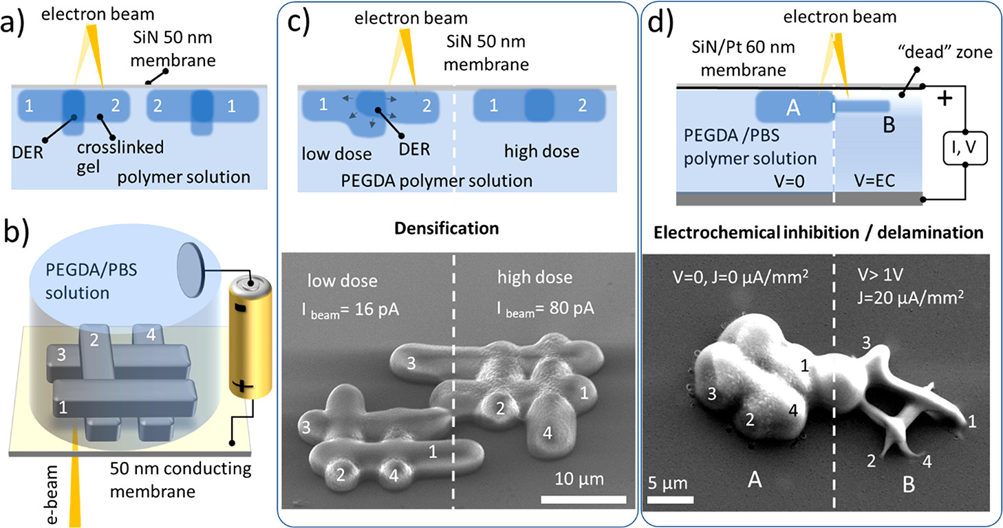
Focused electron beam-induced deposition (3D-FEBID) represents a more innovative 3D printing approach and uses an electron beam to separate the surface of gaseous metal-containing precursors. The experimental technique is capable of creating objects at an ultra-high-resolution but at the cost of being considerably slower than conventional methods.
Similarly, significant progress has been made in the development of deep X-ray lithography, which uses zone plate-focused beams for the precise fabrication of high-aspect-ratio microstructures. The advanced production process causes reduced radiation damage, and this has allowed it to be used within medical applications such as polymerization inside live systems.
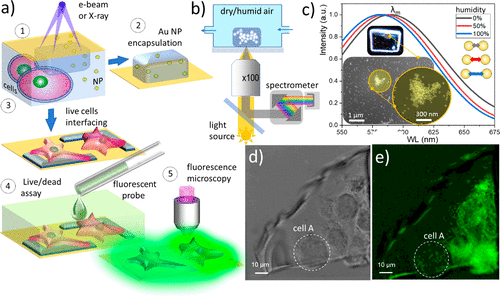
Unfortunately, X-ray oriented methods have drawbacks too. At present, the short wavelengths emitted by X-ray beams can only operate in a vacuum, so the liquid in each chamber could evaporate rather than forming a gel. In order to overcome this limitation, the team theorized that using a thin electron-transparent barrier, they could prevent the liquid from evaporating, while allowing the beam to penetrate the gel.
The NIST team’s gel-based 3D printing method
To effectively deliver focused electron and soft X-ray beams to their liquid solution, the researchers designed a set of closed, fluidic chambers. The devices were equipped with 30–50 nm thin silicon nitride (SiN) membranes, which acted to isolate the liquid from the vacuum of the microscope.
During testing, the chamber was filled with poly(ethylene glycol) diacrylate (PEGDA) 20% w/v aqueous solution, and nine identical membrane windows. By varying only one of the beam’s parameters such as its energy, intensity, step-size, or dwell time, while keeping others locked, the barriers were used to create parts with a range of different feature sets.
After rinsing off the uncured solution, the team used an Atomic Force Microscopy (AFM) to inspect their cross-linked structures. By comparing the height of the sample objects in their hydrated and dry states, the researchers were eventually able to print them consistently and to estimate the size of the gel-based objects without directly measuring them.
What’s more, the method proved capable of producing structures that were 100-150nm wide, leading the researchers to surmise that it could be used for creating computer–brain interfacing devices. In order to test the live-cell interfacing capabilities of their novel technique, the team conducted a further experiment, which exposed SiN membrane cells and a PEGDA polymer to an electron beam.
Although some of the cells died, the majority were successfully integrated into an electrode. As a result, the team concluded that their method had the potential to be used in creating futuristic microscopic implantable devices, at sizes as small as 50nm. “We’re bringing new tools – electron beams and X-rays operating in liquids – into the 3D printing of soft materials,” concluded lead researcher Andrei Kolmakov.
Additive manufacturing on a nanoscale
Given the range of potential uses that exist for nanoscale 3D printed objects, it’s hardly surprising that scientists have sought to optimize the technology in recent years, and produce ever-smaller objects.
Researchers from the University of Dayton have developed an enhanced, cost-effective method of 3D printing nanoscale structures. The Opto-Thermo-Mechanical (OTM) nano-printing technique proved capable of printing at a scale of less than 100nm.
Scientists from the Fraunhofer Institute for Microengineering and Microsystems (IMM) are developing a novel process using multiphoton lithography to create nanoscale metal 3D printed structures. Through the project, the team is aiming to fabricate parts with smaller features than those produced using Direct Energy Deposition (DED) processes.
A team from the California Institute of Technology (Caltech) have used a two-photon lithography method to 3D print metal structures that are no larger than 100nm. The technique is reportedly capable of making metal features that are “an order of magnitude smaller” than any other metal fabrication process.
The researchers’ findings are detailed in their paper titled “Electron and X-ray Focused Beam-Induced Cross-Linking in Liquids: Toward Rapid Continuous 3D Nanoprinting and Interfacing using Soft Materials,” which was published in the ACS Nano journal. The paper was co-authored by Tanya Gupta, Evgheni Strelcov, Glenn Holland, Joshua Schumacher, Yang Yang, Mandy B. Esch, Vladimir Aksyuk, Patrick Zeller, Matteo Amati, Luca Gregoratti, and Andrei Kolmakov.
Nominations for the 2020 3D Printing Industry Awards are still open, let us know who is leading the industry now.
The fourth edition of the 3D Printing Industry Awards Trophy Design Competition is now underway. Enter your design for the chance to win a CraftBot Flow 3D printer.
To stay up to date with the latest 3D printing news, don’t forget to subscribe to the 3D Printing Industry newsletter or follow us on Twitter or liking our page on Facebook.
Are you looking for a job in the additive manufacturing industry? Visit 3D Printing Jobs for a selection of roles in the industry.
Featured image shows a diagram of how the NIST researchers’ new nanoscale 3D printing method works. Image via the ACS Nano journal.