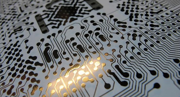
The Israeli-based 3D printing company Nano Dimension has been pioneering the field of 3D printed electronics for quite some time now. Last month, they partnered with 3D printing service provider FATHOM to bring their PCB printer, the DragonFly 2020, to the public eye. The company, which recently got listed on the NASDAQ, has come a long way in research and development with electronics 3D printing, and it seems that the innovative spark is still there. A couple of days ago, Nano Dimension filed a patent application with the U.S. Patent and Trademark Office, which detailed their new process for 3D printing electronic circuit printing, which works by simultaneously curing and sintering two types of ink, conductive metal ink and insulator ink.
“The current standard curing and sintering approach uses a number of different systems to cure and sinter the inks,” Nano Dimension writes in their blog. “Each such system adds cost and complexity, while this new approach has the potential to reduce both.”
With this newly patented technology, Nano Dimension hopes to reduce the number of critical systems within their 3D printers, which will lead to lower production costs, increased speed and reliability, and a less bulky hardware system. “The current standard curing and sintering approach uses a number of different systems to cure and sinter the inks,” Nano Dimension said. “Each such system adds cost and complexity, while this new approach has the potential to reduce both.” In order to reach this new approach, Nano Dimension utilized unique chemically-composed conductive inks that were manufactured within their own laboratory. These inks are engineered with nanoparticles that absorb radiant energy, which creates plasmonic waves on the surface of these nanoparticles.
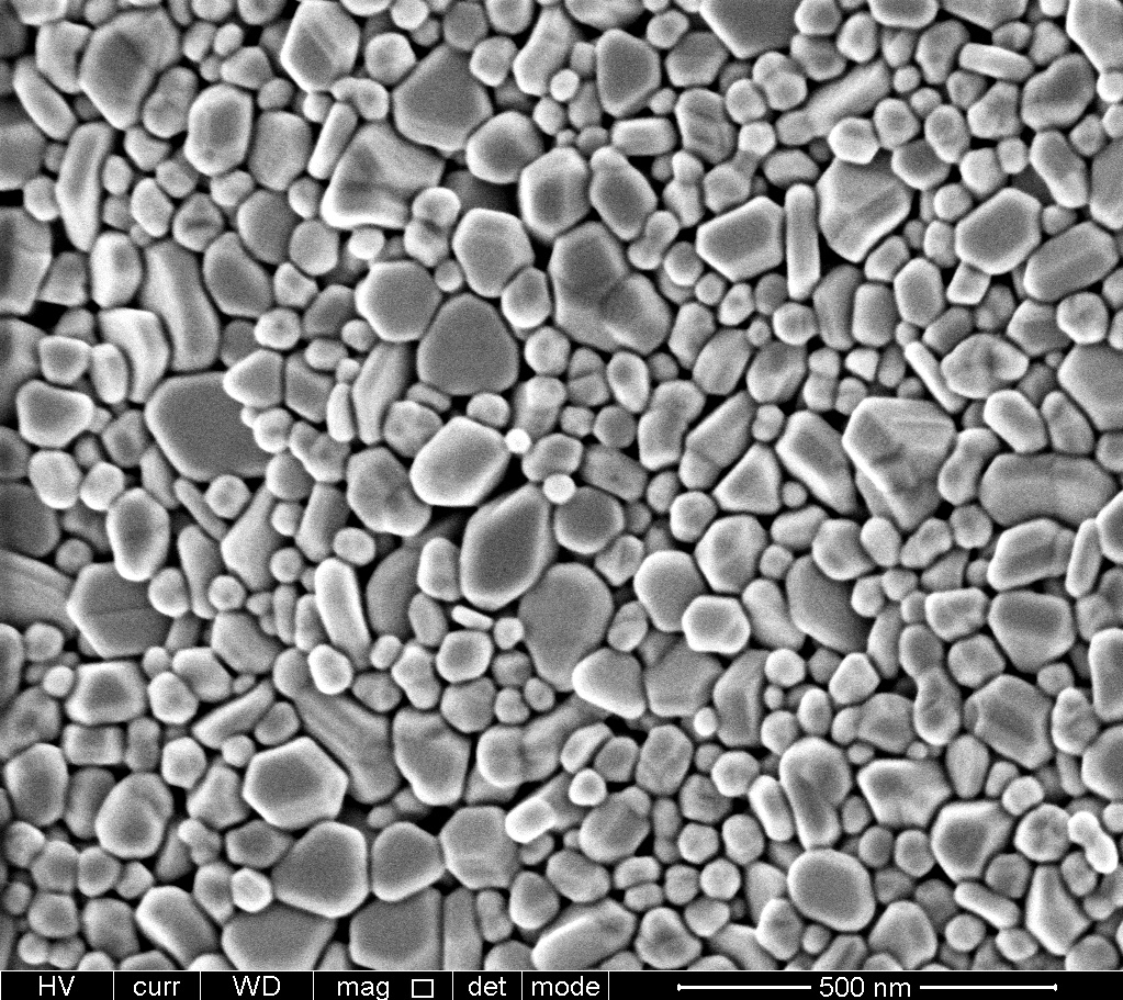
As soon as these plasmonic waves are formed, they’re immediately converted into heat, and the high surface energy creates a fusion of the silver nanoparticles. Using this unique sintering process, Nano Dimension is able to achieve a final uniform metallic trace. Using the radiation emitted from their electronics 3D printing technology, the photoinitiated insulating ink is instantaneously cured, and showcases great mechanical strength and high thermal resistance.
Since 2012, Nano Dimension has been paving the path for 3D printing electronic circuits, and seem set to send a spark through this expanding field with their newly patented technology. By implementing simultaneous sintering and curing, future electronic 3D printers have the potential to be more affordable, faster, and more reliable than ever before.