
German electronics 3D printing specialist InnovationLab has come up with a lower-cost, more environmentally-friendly way of creating Printed Circuit Boards (PCBs).
Developed as part of the ‘SmartEEs2’ EU Horizon 2020 project, the process enables the production of solderable copper circuits, while using less energy than traditional methods and avoiding the need for toxic etchants. Using the technology alongside partner ISRA, the firm is now said to have developed prototype PCBs, which could serve as a basis for a new generation of flexible, wearable electronics.
“This is a state-of-the-art production process, which will decrease costs and reduce logistical dependencies on suppliers while consuming fewer materials, using less energy and producing less waste,” said Dr. Janusz Schinke, Head of Printed Electronics at InnovationLab. “By the end of this year, we expect to have scaled this process to high volumes, meeting customer demands of a million solderable tracks or more.”
InnovationLab’s PCB R&D drive
InnovationLab is a self-proclaimed ‘one-stop shop’ for printed electronics, with a network of industry and academic partners, via which it’s able to support customers’ R&D efforts. Alongside this offering, the firm has established a portfolio of flexible printed pressure sensors, including its BaMoS EV battery monitor, and accompanying SensorMatrixLAB software and TAeTTOOz 3D printing material.
According to InnovationLab, the technology behind its ‘organic electronics’ reduces the steps behind production from nine down to just two. As such, the process is less time, cost and material intensive. The company also says 3D printing opens up a broader material palette than traditional PCB production, including flexible, biodegradable substrates, making it an ideal basis for creating novel wearables.
Elsewhere, through its LAB-2-FAB service, InnovationLab offers to help customers hailing from the consumer, automotive, healthcare industries and more, bring 3D printed electronics ideas from the design into production. This offering is bolstered by the firm’s Tech-2-Market consultancy package, as well as its infrastructure plans, in which it hires out its facilities in the Rhine-Neckar region at a flat rate.
While the company has traditionally acted as a facilitator of 3D printing innovation, it has itself now reached out to the SmartEEs2 consortium, to ramp up its PCB R&D, by working with partners such as the CPI, VTT Technical Research Centre of Finland, TNO, Fraunhofer FEP, Organic Electronics Saxony, eurecat and CENTI.
EU-funded electronics innovation
Over the last two years, the SmartEEs2 program has sought to help European businesses accelerate their testing, experimentation and production of flexible electronic devices. Made up of 14 partners and coordinated by France’s CEA, the project has involved inviting test proposals from qualifying businesses, with those chosen being awarded support and invited to join its pan-EU research network.
Thus far, operating as one of the EU’s Digital Innovation Hubs, the €8 million initiative has focused on helping companies digitize, and enhancing the competitiveness of European firms developing novel electronic devices. With the project set to end later this year, it has targeted a total of 44 application experiments, one of which has reportedly yielded InnovationLab and ISRA’s PCB 3D printing breakthrough.
Compared to traditional PCB production processes, InnovationLab’s is said to run at a lower temperature of around 150ºC, thus making it more energy efficient. The multilayer metal and dielectric printing method also involves depositing material onto a substrate that’s fifteen times thinner, enabling users to reduce their material consumption and waste.
Thus far, utilizing this technology, the firm has managed to create a low-power temperature sensor, NFC communication interface via a printed antenna and a compact solar-powered battery. With the devices having reached a target functionality in testing, their developers now say the process behind them has the potential to enable sustainable PCB production and further hybrid electronic R&D.
3D printing in Flexible Hybrid Electronics
Although 3D printed PCBs haven’t disrupted the traditional electronics market just yet, the technology continues to be the subject of intense research. As recently as March 2022, NextFlex poured $17 million into electronics 3D printing R&D, with beneficiaries like GE Research and Lockheed Martin now using the funding to develop 3D printed radio frequency (RF) and hypersonic flight-related parts.
In more commercial applications, Nano Dimension’s DragonFly IV 3D printer continues to offer users the ability to create highly-complex PCBs in a one-step process. That said, the system hasn’t really achieved widespread adoption, and while the firm’s revenue rose from $811,000 to $10.4 million between Q2 2021 and 2022, this was largely due to a string of acquisitions it finalized over the last year.
Earlier this year, nScrypt’s research arm Sciperio also announced that it had made a potentially significant step with its Factory in a Tool electronics 3D printing system. Sciperio patented an electronic 3D printed personalized therapy device, capable of sending patient data to a video game for therapeutic training purposes.
To stay up to date with the latest 3D printing news, don’t forget to subscribe to the 3D Printing Industry newsletter or follow us on Twitter or liking our page on Facebook.
For a deeper dive into additive manufacturing, you can now subscribe to our Youtube channel, featuring discussion, debriefs, and shots of 3D printing in-action.
Are you looking for a job in the additive manufacturing industry? Visit 3D Printing Jobs for a selection of roles in the industry.
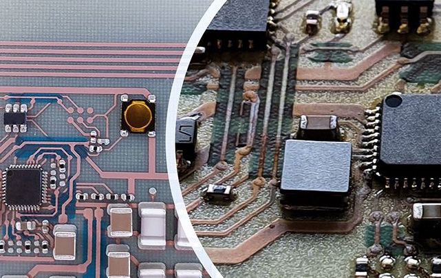
Featured image shows an InnovationLab 3D printed PCB. Image via InnovationLab.