
Additively manufactured electronics (AME) provider J.A.M.E.S (Jetted Additively Manufactured Electronics Sources), has launched a new website to demonstrate and promote knowledge of AME technology.
As per J.A.M.E.S, the AME platform has been developed based on valuable feedback from industrial partners, users, and enthusiasts. The new website has been improved to be more intuitive, user-friendly, and informative.
“Our goal is to create a comprehensive platform that brings all our partners in one place, enabling them to showcase their strengths and promote themselves easily. We strive to concentrate on news and articles centered around 3D printing electronics to provide information. In addition, the community members can share their knowledge and research outcomes while staying in touch with our partners,” said Andreas Müller, the CEO of J.A.M.E.S.

Enhancing AME technology expertise
The primary goal of introducing the new website is to engage a broader audience and promote awareness of the latest progress in 3D printed electronics and AME technology. Additionally, the website will feature novel designs that highlight the “state-of-the-art advancements” in the portfolio of AME applications. In line with J.A.M.E.S’s mission to make AME technology accessible to everyone, the layout of the website reflects a “commitment” to simplifying intricate concepts and providing a user-friendly interface to benefit the users.
The newly launched website by J.A.M.E.S offers a range of features that deliver various advantages for both partners and users. Positioned as a frontrunner in the development of AMEs, the platform allows partners to effortlessly exhibit their products and technologies, says the company. It aids in granting them increased visibility among professionals in the AME industry. Users have access to various information resources such as news articles, publications, and tools dedicated to 3D printing electronics. J.A.M.E.S believes this renders the website as an “indispensable source” for staying updated on all AME-related information.
“Our ultimate objective at J.A.M.E.S is to become the primary point of contact for AME by creating a perfect tool that allows everyone involved in pushing the AME technological advancement forward together seamlessly,” added Müller.
Establishing J.A.M.E.S and scaling AME technology
Founded in 2021, J.A.M.E.S is a joint venture entity powered by 3D printed electronics manufacturer Nano Dimension and military sensor specialist HENSOLDT. To facilitate the progress of 3D printed electronic components, the two companies jointly invested $6 million in this venture, which is headquartered in Taufkirchen, Germany. The primary aim of J.A.M.E.S is to cultivate a community of electronic designers who can freely exchange designs and methodologies related to the manufacturing, integration, and materials of AMEs. Additionally, the joint venture offers prototyping services and AME applications to both its community members and users from various industries.
Nano Dimension worked with communications technology firm L3Harris on a project that utilized AME technology. The collaborative efforts focused on utilizing 3D printing technology to produce a radio frequency (RF) circuit capable of transmitting data to and from the International Space Station (ISS). Typically, the conventional production of RF circuits involves a lengthy and iterative trial-and-error process. However, by leveraging Nano Dimension’s AME technology, the partners successfully 3D printed a 101 x 38 x 3mm circuit within approximately 10 hours. Subsequent testing conducted by L3Harris, compared the performance of the 3D printed RF circuit to that of a conventionally manufactured counterpart, revealing similar transmission capabilities between the two. Notably, the advantages of 3D printing became evident in terms of time and cost efficiency. Nano Dimension’s RF circuit enabled swift design iterations, significantly reducing costs and expediting the time required to bring the product to market.
What does the future of 3D printing for the next ten years hold?
What engineering challenges will need to be tackled in the additive manufacturing sector in the coming decade?
To stay up to date with the latest 3D printing news, don’t forget to subscribe to the 3D Printing Industry newsletter or follow us on Twitter, or like our page on Facebook.
While you’re here, why not subscribe to our Youtube channel? Featuring discussion, debriefs, video shorts, and webinar replays.
Are you looking for a job in the additive manufacturing industry? Visit 3D Printing Jobs for a selection of roles in the industry.
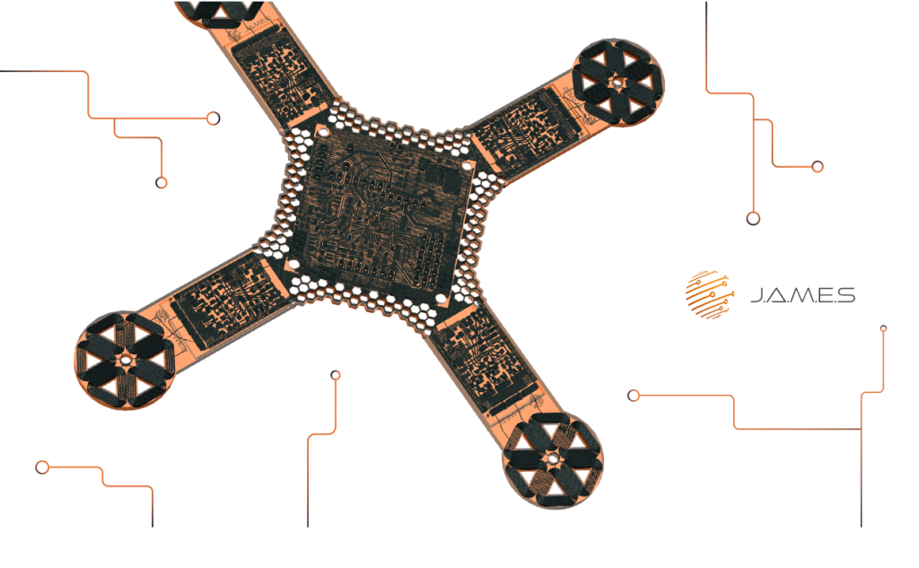
Featured image shows zoom-in view of 3D printed electronic by J.A.M.E.S. Image via J.A.M.E.S.