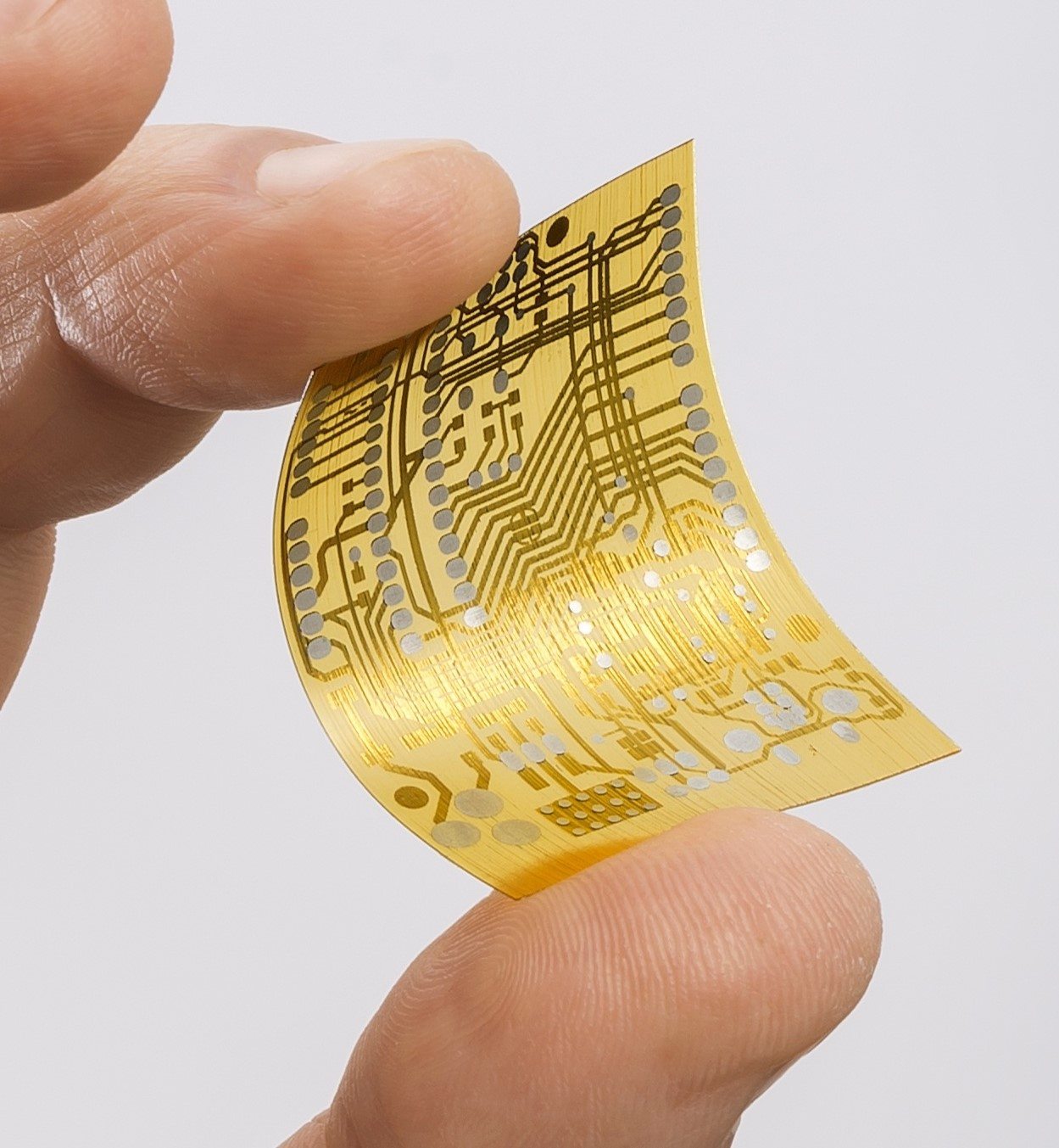
Fresh off the heels of their latest development in software packaging, leading tech company, Nano Dimension have just made another announcement guaranteed to improve the overall performance and speed of developing printers. Dedicated to providing companies with in-house abilities to print complex multi-layer circuit boards, Nano Dimension is constantly developing inkjet technology to be used in combination with their innovative printers across industries. In their latest feat, Nano Dimension has filed a patent application with the U.S. Patent and Trademark Office for the development of a new nanometric conductive ink based on a unique synthesis.
Smaller particles yield better performance capabilities
The patent would protect a new nanoparticle synthesis process capable of shrinking the size of silver nanoparticles in ink products down to an unheard of 4 nanometers. With precise control of the size and surface of nanoparticles, developers hope to improve performance of the company’s DragonFly 2020 3D printer, which is still in its development stages. Overall, the innovative new ink will potentially allow for:
- Lower melting temperatures
- More complete sintering (fusing of particles into solid conductive trace)
- Higher levels of conductivity
More groundbreaking features
Nano Dimension posits that the ink will also dramatically accelerate printing speeds in new printers. This will therefore enable users to save ink for the 3D printing of electronics such as printed circuit boards, antennas and more.
About Nano Dimension Ltd.
Nano Dimension, founded in 2012, focuses on development of advanced 3D printed electronics systems and advanced additive manufacturing. Nano Dimension’s unique products combine three advanced technologies: 3D inkjet, 3D software and nanomaterials. The company’s primary products include the first 3D printer dedicated to printing multi-layer PCBs (printed circuit boards) and advanced nanotechnology-based conductive and dielectric inks.To learn more about Nano Dimension, head over to their website.
Be sure to sign up for the 3D Printing Industry newsletter to stay up to date with all the latest information!