After the International Conference on AM & 3DP in Nottingham last week, I wrote up my review of the event and the story that has generated the most interest and the most questions — by far — is that pertaining to the new “materialization” process highlighted in a presentation from Mark Tilley of Architected Materials. The presentation was entitled “3D manufacturing at the Speed of Light”. I, and a few others, prior to the session were working on the assumption it was a faster than normal DLP process and it would likely be quite interesting.
We were off the mark, and I mean WAY off. This was not about a tweak here and an improvement there with a process that we are familiar with — this is something totally different. Completely new. No one I have spoken with subsequently has ever seen anything like this before. With the exception of event organizer and 3D printing guru Phil Reeves, who had been privy to the process in action in the secret US labs — where it has been under development since 2007 — and hence why Mark was presenting at the conference.
There were (and still are really) questions a plenty — who, where, why, what and how to start with. I’ll start with what and how, but please bear in mind that this is still new to me too — and while I am sure many of you will “get” the science, my poor brain is still struggling with it.
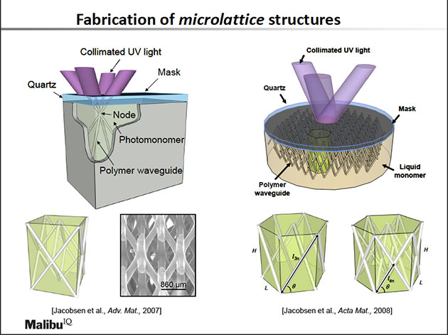
So what are we talking about here? Well, as I stated in the review, this is a resin process developed as “a new 3D manufacturing technology” according to Mark. The process has been developed by Alan Jacobsen, who holds a number of patents around it. In some ways, due to its nature, it does have similarities with the SL / DLP 3D printing processes — the vat of resin, the light/heat source required to cure it, the ability to produce complex structures. But there the similarities end. The resin material is a photomonomer, the light source is ‘collimated UV light’, the collimation being absolutely key to the process, and it is directed into the resin in a single pass, through a mask with thousands of small holes, and a layer of quartz, to form self-propagating photopolymer waveguides, that in turn form micro lattice structures.
As both Phil and Mark explained to me (it took multiple goes to sink in): “as the collimated light passes through the pin hole it causes the resin to cure. As the material cures, the light passes or propagates down the solid material – which acts as a wave guide, allowing the light to pass further and further into the liquid.”
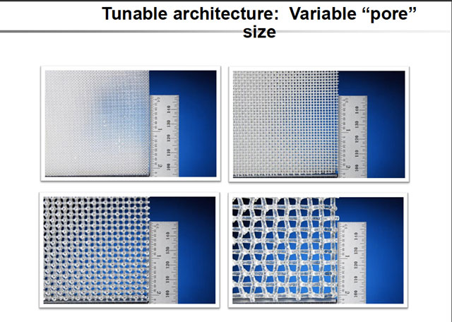
The structures can be pre-determined in that the process can produce lattices that range in pore size (according to the size of the holes in the mask) and properties including highly flexible and elastic to rigid and stiff.
Once set up, the actual materialization process takes 30 seconds from introducing the light source to solid part. A staggering speed of production that boggles the mind, particularly when you are used to dealing with the time-scales of “traditional” 3D printing.
But there are limitations to this process — serious ones for anyone thinking they can get their hands on this and produce any thing and every thing their hearts’ desire. The nature of the process means that the Z-axis is hugely restricted, again, this is in the context of “traditional” AM/3DP processes. The maximum Z-axis height is around an inch and this is due to the system set up and how far the UV light can be projected successfully into the resin. The second limitation is the materials — resins, while improved since the origins of stereolithography, still suffer from degradation and discoloration over time, and particularly if exposed to sunlight.
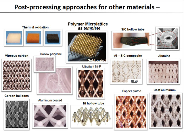
However, the resulting lattice structures have undergone intensive research in terms of secondary processes – plating and casting operations, with a wide range of materials, have all had positive results.
There are some obvious ‘whys’ — this is a very fast, scalable process (the process itself and volumes of parts produced) that can be applied in many areas: notably for impact protection, heat transfer applications and stiffened structural composites. Automotive and aerospace applications in particular are top of the agenda — hardly surprising considering the backers (see below). There are many other applications too, probably some that haven’t been thought of yet. But this is because the process — currently without a definitive name — is still developmental although it is well on the way to commercialization.

As I mentioned above, the R&D into this process has been extensive and onging for more than six years. The top-secret nature of HRL has ensured it has been kept under wraps — until now that is. Architected Materials is the new start-up company (Mark is the CEO) that has been set-up to take the process to commercialization backed by MalibuIQ. The current status is that a pilot plant is being made ready on the HRL campus. Mark was telling me about some of the trials and tribulations involved, but even so, he could not contain his enthusiasm and ambitions for Architected Materials and how far this can go.


