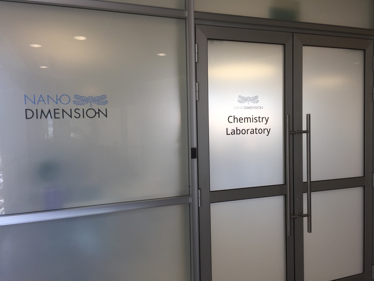
I realize that I increasingly tend to use hyperboles to describe my direct experiences with some of the technologies that are being introduced in the 3D printing industry. Like XJet and Massivit before it, after seeing it in person, I can confirm that Nano Dimension’s approach to 3D printing electronics could truly be a revolutionary step forward in PCB’s, a sourly needed one indeed.
I had planned my visit to the Tel Aviv tech hub with the intention to visit 3 companies in particular and they all confirmed my expectations: these are the technological biggest innovations I have seen in an industry that, recently, has been evolving and optimizing processes more than inventing entirely new ones. While they do build on Objet’s polyjet (inkjet) experience, these 3D companies bring about bigger innovations than any other I know in the world of 3D printing. XJet for metals, Massivit for large size prints and Nano Dimension for electronics.
Both XJet and Nano Dimension owe their innovation to the advancement of material science and nanotechnology. There is still a lot to be done but there is little doubt that combining nanotechnology and 3D printing technology, two of the hottest tech sectors of the past 20 years, can only bring about amazing new possibilities. While XJet targets metal manufacturing, NanoDimension wants to bring about revolution in electronics and in all that concerns upcoming IoT applications.
I’ll be the first to admit that I know very little about electronics. I do however realize that today’s PCB’s are still way too similar to yesterday’s PCB and no true innovation, not even real IoT products, can exist until we find a new and much more efficient way to make them. Simon Fried, CMO, Co-Founder & Member of the Board at Nano Dimension,whom I met with during my visit, believes Nano Dimension is the first to develop that new way. Judging by what I saw, I believe him.
Some say that the process used by Nano Dimension is not really 3D printing. It isn’t in that it does not make actual objects (now) but it is for just about everything else. First of all it is intended to be used as rapid prototyping technology. “Current PCB prototyping methods are antiquated at best,” Simon explained, “engineers have to design them layer by layer and then somehow explain the manufacturers in China how to put them together. This is a very time consuming, expensive and risky procedure, which stifles innovation. Having a local printer which could enable an engineer to rapidly and affordably test a few different prototypes would be a game changer.”
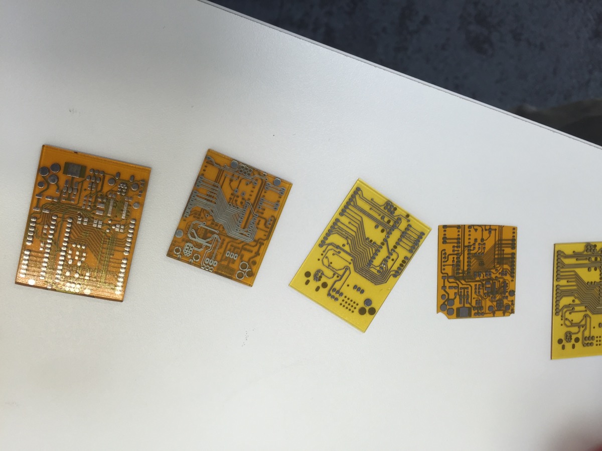
This is the same concept of rapid prototyping at any level, but with electronics it certainly assumes a whole new dimension. The other way that Nano Dimension’s technology is similar to 3D printing is that it is a 3D inkjet process, just like polyjet. Objet’s trademark technology – which is a direct derivation of 2D digital printing technologies and it is also the most highly engineered technology in all of 3D printing – is the only one able to do multiple materials with high precision. Nano Dimension takes this to a new level by combining a polymer material with a conductive metal nanomaterial (in this case silver) in the same print job.
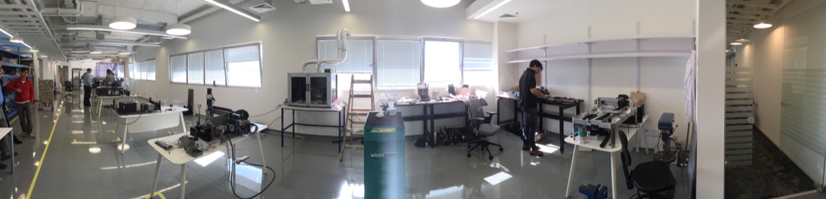
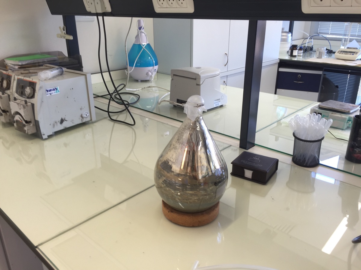
This creates an enormous new level of complexities: both materials need to be cured together; the polymer needs to be able to contain the heat deriving from the metal’s high conductivity, they need to be layered and, if this technology will ever be used for actual production (which is one of the company’s medium and long term goals) they will need to be stable enough. All this requires significant advancements in materials science (as does most 3D printing, in fact), so one of the primary activities at Nano Dimensions – even more so now that more funding has been obtained – takes place in the chemical laboratories.
One day 3D printed PCB’s will be flexible, geometrically complex, full 3D dimensional and fully functional objects. The idea is not so different from Voxel8’s 3D printer, only, instead of extrusion, it uses high precision (and highly scalable) piezoelectric inkjet print heads for a highly industrialised process. This does not mean that the technology will not enable Arduino-like low-cost PCB’s. In fact it may be just the opposite. The main difference is that instead of having them manufactured in China you might just have to go to your friendly professional 3D PCB printing service in your area.
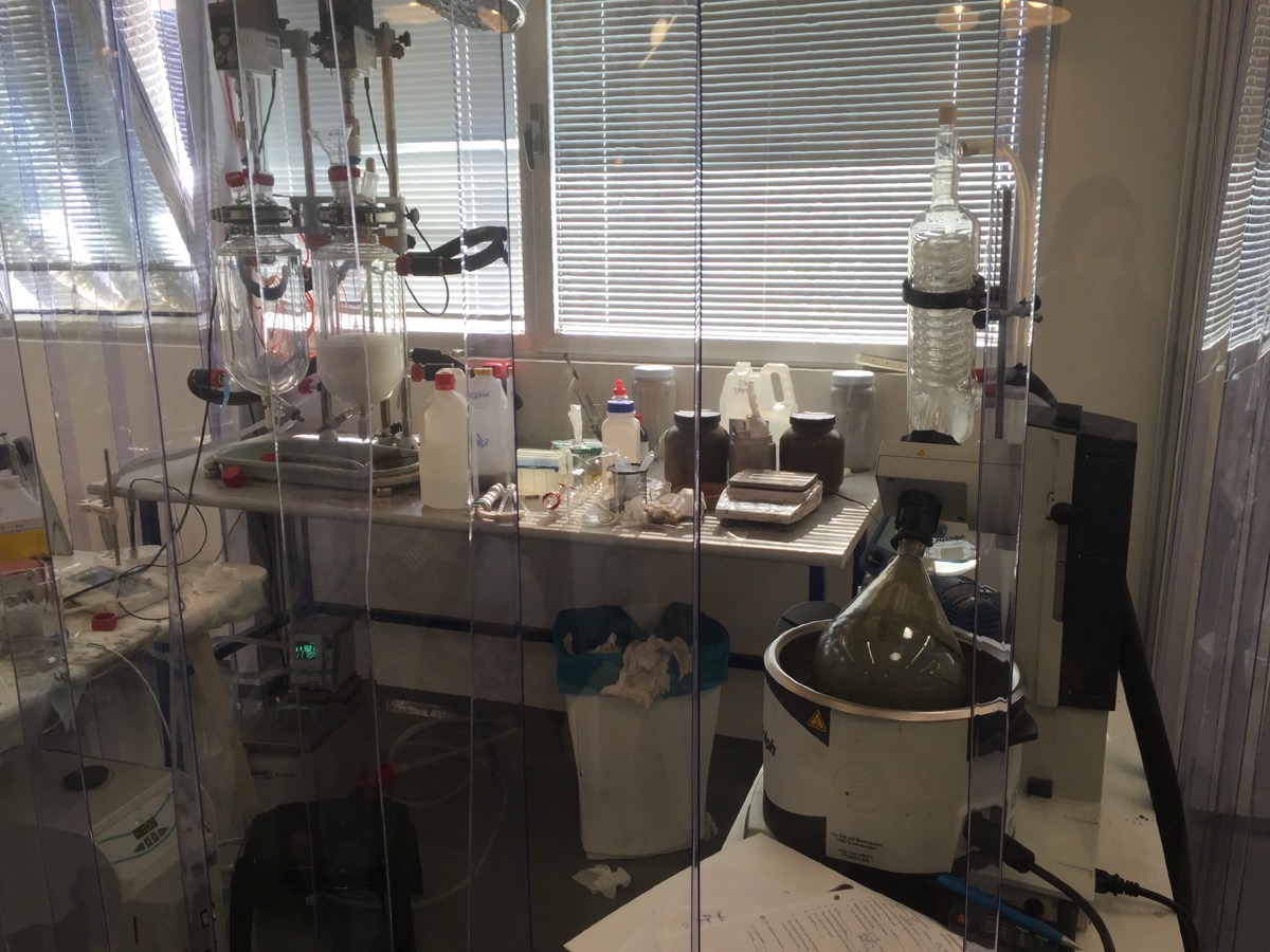
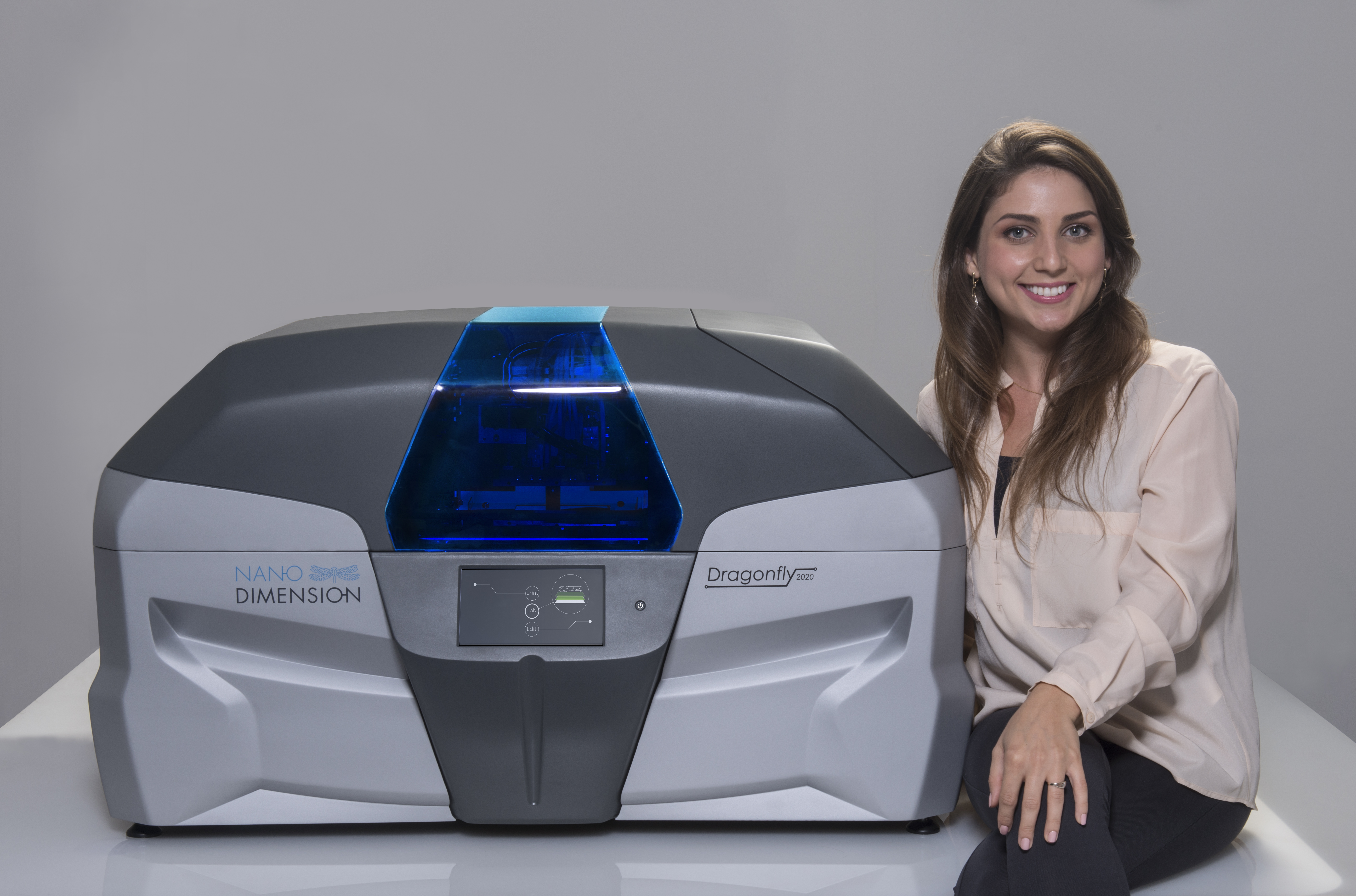
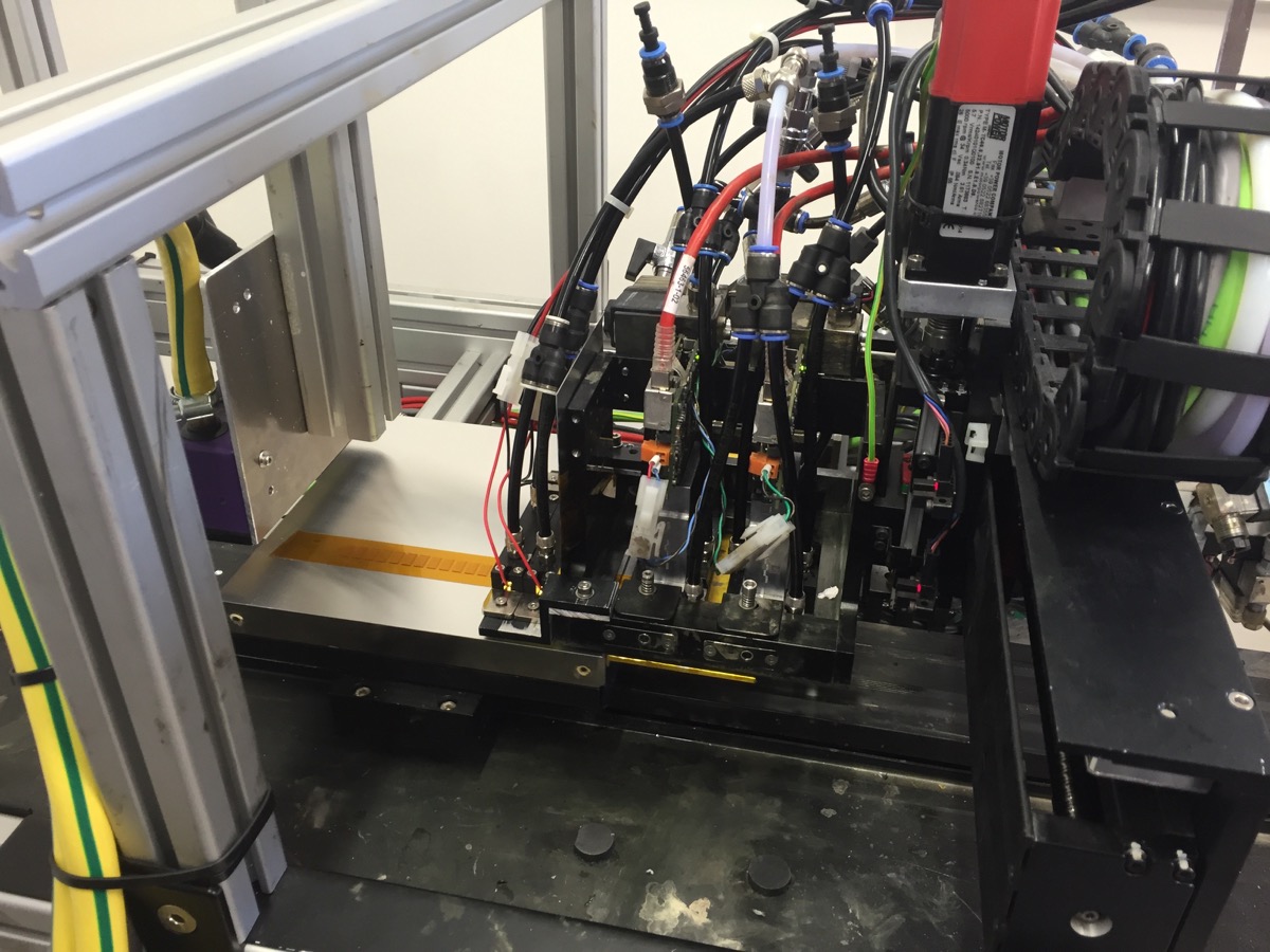
The metallic silver nanoparticles are extracted from salt through a proprietary process. The polymers are also developed in house. When I visited you could see that the entire company is in the middle of a very strong and rapid expansion phase. The newest version of machine has just been completed and exhibited at the recent printed electronics show in California. It is soon going to be shipped to the first beta customers, with the commercial launch planned for a year from now.
I could only see the earlier prototype versions but, judging by the photos, it looks like it is moving fast. In-house designer Lena Kotlar spent countless hour to create Nano Dimension’s DragonFly 2020 printer, using the the speed and presence of Lamborghini’s Aventador and the delicate functionality of a dragonfly’s wings as inspirations. This made me think of another interesting trend: XJet, Massivit and Nano Dimension are very much focusing on the aesthetic of their machines. They all developed a first functional prototype and then a final version where the exterior shows their machines for what they are: the very fast moving future of manufacturing.