
Something that never ceases to amaze me about 3D printing is how similar technologies can be applied to so many different fields and areas of expertise. So it happens that, while we are wandering around the Inside3DPrinting stands during the Berlin event, we can be amazed by the size of a real life BigRep One machine and, just a few stands away, be truly baffled by nano-size 3D printed objects.
Nanofabrication is what Nanoscribe, a spinoff of the Karlsrhue Insitute of Technology (KIT), does: it applies stereolithography to the nanoscopic word. Just to give you an idea of what that means, when we talk about FFF we have resolutions of as low as about 100 micron. Here 100 micron is the size of the objects. And to make that even clearer, when we talk about highly accurate SLA and DLP machines, we get into the picometer range resolution. With Nanoscribe’s Photonic Professional GT machine, the resolution for objects as tall as one centimeter is 1/1000th of that.
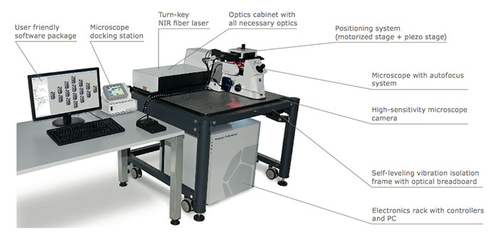
The Photonic Professional GT system, which, as Michael reported, was introduced in the beginning of last year, is now available commercially (hence the company’s presence at the show). It does not just offer the higher resolution imaginable (without falling into the highly complex real of subatomic quantum physics and its inherent uncertainty), it also does two things that make it accessible to a wider audience (of highly specialized scientists): ease of use and high speed 3D printing.
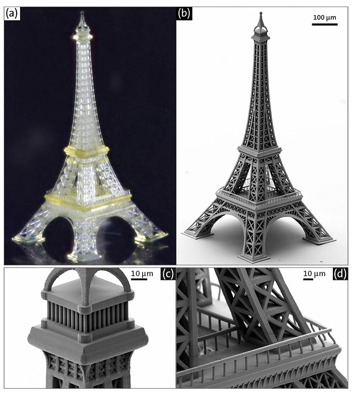
While the first is achieved mainly through intuitive software, that we will discuss further on, the second utilizes a Galvanic mirror system (which is basically a system that regulates mirrors in laser applications to speed up the laser processes) which has made it possible to increase 3D printing times by two order of magnitude, with minutes turning into seconds. Because of its speed, the Photonic Professional GT can be used to create large size objects which, in this case, means objects as large (or as tall) as one square centimeter, such as this Eiffel tower replica, the smallest offer built.
The technology used to 3D print at a nanoscale is called Two Photon Polymerization or Two Photo Lithography (the two terms are interchangeable) and was brought to international media attention in the beginning of 2012 by a team at Vienna University.
It is very similar to regular stereolithography, except that it uses femtosecond laser pulses (a femtosecond is 10 to the -15th seconds or 0,000000000000001 seconds) to cure the polymers at the nanoscopic level). You may think this is just a very cool experiment and has no real life applications but in that case you would be macroscopically wrong.
Nano is huge
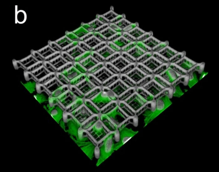
For a long time nanotechnology has been confined to the range of those things that will probably happen in the future. Now there is so much nanotechnological material around us that it is almost commonplace. The same is now happening for commercial nanofabrication. The ability to 3D print nano-scale Photonic Wire Bonds (PWB) will allow computer scientists to overcome communication bottlenecks in data centers and high performance computers. In biotechnology nano-scaffolds are making it easier than ever to grow all types of living cells. Nanofabrication will have applications in the development of mechanical metamaterials and of new nano-shaped surfaces that will, for example, replicate a Gecko’s setae, giving any one and any object Spider-man like climbing (or clinging) abilities. Another application is in filtration systems: with Nanoscribe’s machine it is possible to create nanofluidic filters inside channels that are only a micrometer wide.
To give scientists access to its machines without having to get into their complex workings, Nanoscribe has developed a range of software that, just like in any desktop 3D printer, can make all the difference both in quality and accessibility. Nanowrite is an easy to use graphical user while the Nanoslicer software transforms the .stl files into the Photonic Professional GT native data format: GWL. Through the DeScribe software users can edit the GWL files, check them for printability and even monitor the writing process by means of an SEM (scanning electron microscope) connected optical camera. Are you ready for a Nanofablab?
[nggallery id=156]