
Nano Dimension, via its joint venture J.A.M.E.S, hopes to accelerate the use of 3D printed electronics. Earlier this year, the company gathered users of what it terms Additively Manufactured Electronics at its Munich office where I interviewed the attending panelists.
Dr. Filip Granek, the CEO of XTPL, a company working on “deep technology for additive manufacturing of electronics.” Granek believes printed electronics have a wide range of applications, including displays, semiconductors, advanced PCBs, biosensors, and anticounterfeiting.
Their primary focus is refining the resolution to make features as small as “one micrometer, so roughly 100 times smaller than the width of the human hair,” remarked Granek. XTPL’s focus is on ultra-high-resolution dispensing of functional materials, which are relevant to the manufacturing of electronics, including metals, semiconductors, and isolating materials. This leap in resolution, combined with functional materials, is projected to unlock many applications in next-generation electronics, including flat panel displays, advanced semiconductor packaging, and bio-sensors.
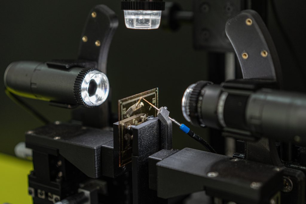
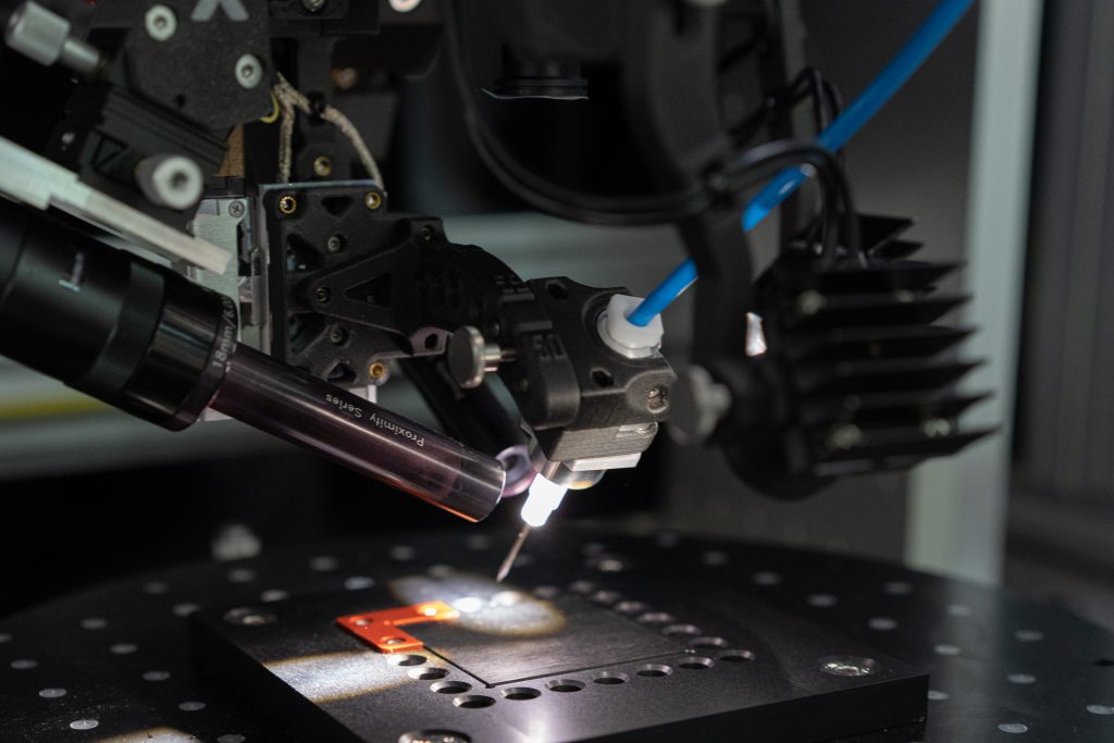
Achieving such precision is no small feat. Granek explained, “Our approach is on dispensing. Pushing functional liquids to a very small nozzle.” He likened the process to “pushing toothpaste through a tube,” emphasizing the use of highly viscous inks and minuscule nozzles that are “as small as one micrometer in diameter.”
Additionally, Granek highlighted the value of their technology when applied to unusual geometries in microelectronics. He observed that microelectronics, at a closer glance, are not flat but have a “highly complex topography.” “On the microscale, direct electronics become very three-dimensional,” suggesting a potential shift in how we perceive and interact with electronics in the future. Granek underscored the challenge and significance of this evolution, emphasizing the need to “write electrical interconnections not just on the horizontal plane, but also on a vertical plane, with good adhesion to both layers.” This capability, he believes, will revolutionize how we design and use electronic devices in the future.
Applications for XTPL’s printing method
Granek gave details on potential applications of their high-resolution dispensing technology in the electronics manufacturing sector. While wearables and medical applications are undoubtedly among the prospective uses, Granek revealed the company’s emphasis is on “novel flat panel displays,” especially those significantly miniaturized and intended to be near our eyes. Such displays not only adopt a three-dimensional shape but also necessitate exceptional resolution. Granek also indicated that another crucial avenue for their technology is in the “domain of advanced packaging in the semiconductor industry,” specifically for “interconnecting individual chips in a three-dimensional mode with a high resolution.”
When prompted on the implications of their advancements in the context of smart factories or the Internet of Things (IoT), Granek acknowledged the possibility but clarified that XTPL’s focus isn’t primarily on end-use. Instead, the emphasis is on “functionality in the production line.” Nonetheless, he envisages this technology being incorporated into “IoT or VR devices.” Granek further highlighted the rising significance of larger chips in artificial intelligence. The increasing size, while providing enhanced computational power, necessitates perfection in every segment. He envisioned their high-resolution dispensing tool playing a pivotal role akin to a “local surgeon” in rectifying imperfections or “defects in the production line,” thereby enhancing production yield and optimizing the value derived from these increasingly expensive larger chips.
The Transition from Lab to Fab
While XTPL’s ambition is transforming the world of microelectronics, its deployment takes a dual-pronged approach. On the one hand, the company offers a “standalone R&D printer” that aids “innovators in Europe, the US, and select major countries” in their developmental and evaluation projects. Conversely, Granek revealed they also possess a “printing engine” that seamlessly integrates with “third-party systems.” Collaborating closely with capital equipment manufacturers rooted deeply in the supply chains of diverse industries like flat panel display, semiconductor, and printed circuit board, XTPL aims to be an integral component of their larger machinery.
However, transitions come with challenges. Reflecting on XTPL’s journey, Granek observed that the company is at a crucial “turning point.” Founded nearly a decade ago, the firm spent most of its years engrossed in technology incubation. Now, as they enter the market, user feedback — both “good” and “critical” — is shaping their course. Granek admitted the current challenge lies in transitioning their technology “from the laboratory environment into the brutal mass production environment of modern electronics.” Making the leap from “lab to fab” isn’t without hurdles, but Granek’s determination to see the company’s vision come to fruition is evident.
Tools and Solutions for Next Generation Manufacturing
In charting the course for XTPL’s next five years, CEO Filip Granek unveiled a twofold strategy. First and foremost, the immediate focus lies in “heavily deploy[ing] our printing modules” and fortifying partnerships with capital equipment sectors. Granek envisions XTPL becoming “a recognized and accepted supplier of high-resolution dispensing solutions” in industries ranging from flat panel displays to semiconductors and printed circuit boards. The ambition continues. Granek emphasizes XTPL’s objective to “become a household name” and envisages its integration into products we will purchase “in the next 2-3-4 years in a major market or the supermarket.”
XTPL will not take its foot off the pedal of innovation. Granek expressed the company’s intent to refine its technology, aiming for enhanced speed and precision to cater to future-generation applications.
Granek voiced enthusiasm for global manufacturing initiatives, particularly highlighting actions like the US’s CHIPS Act and Germany’s investment in semiconductor plants. He sees these movements as an auspicious sign, noting the shift towards repatriating manufacturing to Europe and the US. More than just establishing a manufacturing foundation, Granek views this as an opportunity to bolster “innovators who create tools and solutions for next-generation manufacturing.” Emphasizing the need for sustainable, green, and competitive production, he believes this environment favors XTPL’s growth.
Reducing material wastage?
Highlighting the environmental implications of semiconductor manufacturing, Filip Granek, the CEO of XTPL, sheds light on the potential of additive processes to reduce waste and increase efficiency. In traditional semiconductor manufacturing, the reliance on “subtractive processes” often results in the wastage of rare materials from the Earth’s crust. Granek notes, “to produce fine features, we remove most of these rare materials” only to utilize a fraction of them for specific functionalities.
However, this approach can change with a shift to high-resolution additive solutions. Granek underscores the potential of additive methods, suggesting that “instead of wasting 99% of the materials,” which are extracted with significant energy and carbon footprint, industries can now optimize the use of these rare materials. In the context of a rapidly changing global landscape with constrained access to certain resources, Granek believes efficiency in using these materials will gain paramount importance.
Amid growing global concerns about resource constraints, Granek weighed in on China’s decision to limit exports of two pivotal materials. He predicted, “This is just the beginning of a certain global situation we will face.” Granek emphasizes the rationality of optimizing the use of rare materials, especially when so much energy goes into their extraction and purification. “The reasonable thing to do is not to put a lot of effort to mine rare materials and then waste most of them in the manufacturing process,” Granek remarks, making a case for more judicious resource management.
Furthermore, Granek shines a light on the burgeoning role of additive manufacturing in electronics, indicating its relevance in today’s evolving technological landscape. “There are multiple initiatives and multiple activities in the research area in the industry area where the focus of additive manufacturing in the domain of electronics is becoming a real thing,” he shares, stressing the significance of these developments for next-generation electronics.
Who is leading the industry? 3D Printing Industry Awards Winners.
Read all the 3D Printing Industry coverage from Formnext 2023.
To stay up to date with the latest 3D printing news, don’t forget to subscribe to the 3D Printing Industry newsletter or follow us on Twitter, or like our page on Facebook.
While you’re here, why not subscribe to our Youtube channel? Featuring discussion, debriefs, video shorts, and webinar replays.
Are you looking for a job in the additive manufacturing industry? Visit 3D Printing Jobs for a selection of roles in the industry.
Featured image shows a sample made for Taiwan’s Industrial Technology Research Institute. Photo via XTPL.