Engineers at Tufts University in Massachusetts have used 3D printing and metamaterials to develop novel optical devices.
The research, published in the journal Microsystems & Nanoengineering, demonstrates methods of creating metamaterial embedded geometrical optics (MEGOs) with stereolithography (SLA). These 3D printed structures have the ability to absorb electromagnetic signals from any direction at selected wavelengths.
“The ability to consolidate functions using metamaterials could be incredibly useful to reduce the size of spectrometers and other optical measuring devices so they can be designed for portable field study,” said Sameer Sonkusale, Professor of electrical and computer engineering at Tufts University’s School of Engineering.
3D printed metamaterials for optical devices
3D printed metamaterials incorporate unique properties such as electric and sonic manipulation, as well as pressure-induced shape-shifting. These materials can be fabricated at resolutions down to 200 nanometers, which makes them small enough to process wavelengths of energy, hence its uses in optical and medical devices.
According to the researchers at Tuft’s Nano Lab, 3D printing technologies, such as two-photon polymerization(TPP), and SLA can provide such printing resolution for the fabrication of even finer metamaterials that can detect and manipulate electromagnetic signals, including visible light.
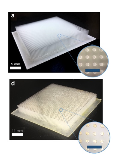
Thus, the team used the Formlabs Form 2 3D printer, metal coating, and etching to create metamaterials with complex geometries for wavelengths in the microwave range. This prompted the creation of a hemispherical device that can absorb electromagnetic signals in any direction at selected wavelengths. This design was based on the eye of a moth, which uses such a function to detect light.
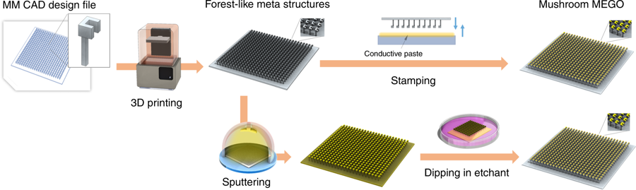
As a result of additive manufacturing, various shapes, sizes, and pattern orientations can be conceived to create MEGOs that absorb, enhance, reflect or bend in an improved manner than conventional fabrication methods.
“The full potential of 3D printing for MEGOs has not yet been realized,” added Aydin Sadeqi, a graduate student in Sankusale’s lab at Tufts University School of Engineering and lead author of the study. “There is much more we can do with the current technology, and vast potential as 3D printing inevitably evolves.”
“We were able to design and implement MEGO devices with unique functionality, one that takes advantage of the large area 3D printing of dielectrics with the embedding of metal patterns.”
The researchers believe that improving resolution in 3D printing will further MEGO devices to reach Terahertz wavelengths for optical frequencies in the near future.
“Three-dimensional printing of metamaterial embedded geometrical optics (MEGO)” is co-authored by Aydin Sadeqi, Hojatollah Rezaei Nejad, Rachel E. Owyeung, and Sameer Sonkusale.
Vote for the 2019 3D Printing Awards.
For the latest academic additive manufacturing research, subscribe to our 3D printing newsletter and follow us Facebook and Twitter.
Visit our 3D Printing Jobs board to find out more about opportunities in additive manufacturing.
Featured image shows the geometry of a moth’s eye provides inspiration for a 3D printed antenna that absorbs specific microwave frequencies from any direction. Image via Hojat Nejad/ Tufts University.