Researchers at the University of Massachusetts Amherst have developed a new 3D printing approach that could serve as a much lower-cost means of creating high-resolution parts than Two Photon Polymerization (TPP).
As opposed to the expensive femtosecond lasers required to cure materials during TPP, the team’s less pricey method involves deploying an LED visible light source, at a significantly lower intensity. Despite this, the engineers’ ‘Triplet-Triplet Annihilation’ (TTA) process is still able to achieve submicrometer feature sizes, hence they say it could now “open the door to low-cost submicron resolution fabrication.”
High-res printing for the people
Even though the researchers have developed their fresh approach as an alternative to TPP, they accept that the latter continues to represent a viable means of 3D printing at extremely high resolutions. Typically capable of producing parts with features 60 to 100 nm in size, TPP machines tend to address applications where precision is key, such as the creation of microfluidic or medical device prototypes.
In practice, such systems achieve this by firing short laser pulses at a photoinitiator-loaded material, in a way that enables it to absorb two photons in a very small volume or ‘voxel.’ It’s the minute diameter of this voxel that lends the technology its extreme accuracy capabilities, but it also tends to rely on the use of femtosecond lasers, which can cost anything from tens to hundreds of thousands of dollars.
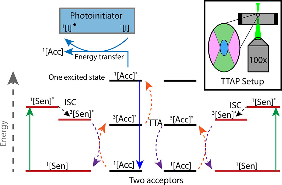
When it comes to replicating TPP’s high-energy transitions using low-energy photons, one approach that has previously shown potential is TTA. However, despite the technology’s seemingly high efficiency under low light intensity, the researchers say that it has only been deployed in photovoltaic, microfluidic photochemical synthesis or photochromic material R&D thus far, not sub-micron 3D printing.
Trialing Triplet-Triplet Annihilation
In their experimental TTA set up, the engineers used a low-intensity LED light source to print a resin made of palladium, octaethylporphine and diphenylanthracene. During initial testing, the system operated by bouncing LED beams off a digital micromirror array to create green light. This in turn, proved capable of triggering the material’s photosensitizer in two places, which, through a process known as ‘intersystem crossing,’ led to the formation of a single light absorption point.
From this point or ‘acceptor,’ light energy was then transported via what the researchers assume was a Förster Resonance Energy Transfer or ‘FRET’ reaction, to the resin’s photoinitiator, causing it to undergo polymerization into samples.
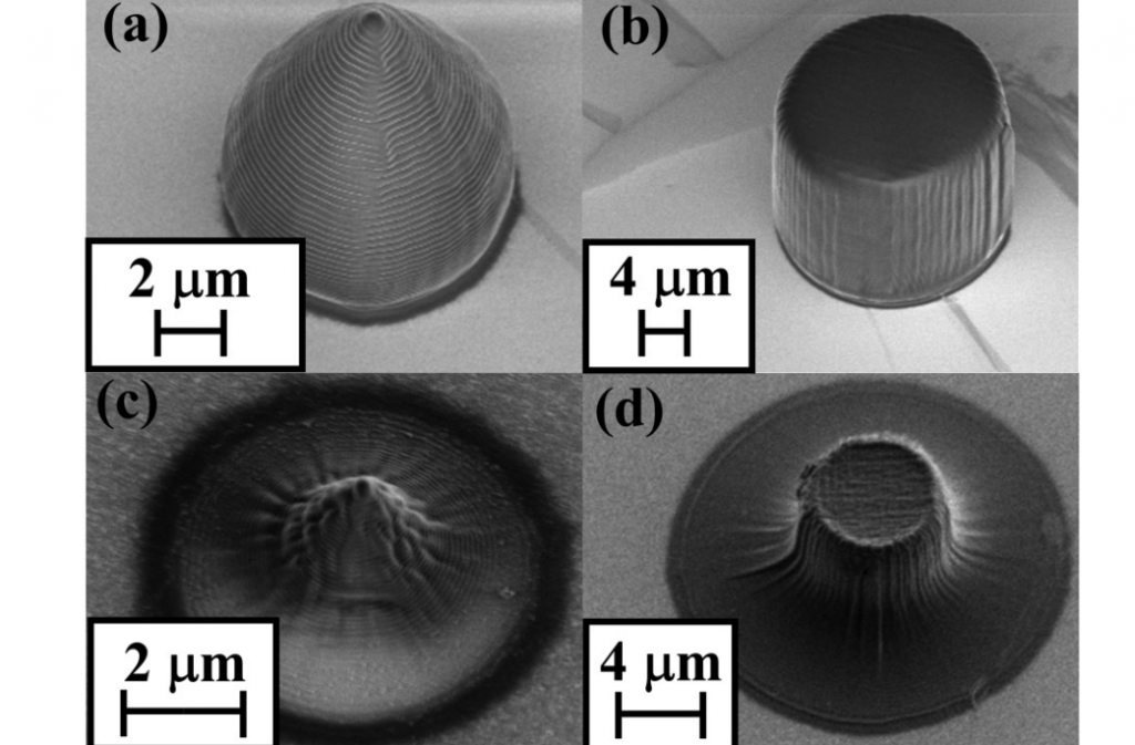
Once they’d perfected this process, the team deployed it to produce parts with features of various different sizes, in order to determine the best resolution possible via TTA 3D printing. These experiments were found to yield consistently sized and shaped square patterns with 0.55 to 4.5 μm sides that, even when created using the least accurate identified parameters, only deviated by up to 0.3 μm.
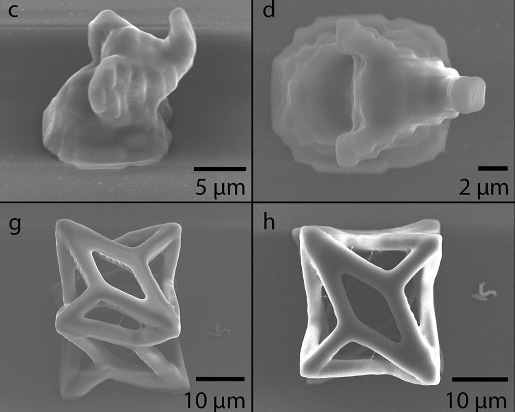
Following some iteration, the team later came up with a motorized stage-based set up, in which voxels were printed one at a time, and the stage was moved to guide light to the next layer. This mechanized approach enabled the engineers to build more complex models, such as strut-like and elephant-shaped structures with suspended features, at an illumination time of less than 0.1 second per voxel.
As a result, the team now believe that their cost-effective approach has the potential to “drive further innovation in the field of high-resolution 3D printing,” and with further development along the lines of light parallelization and bespoke resin formulation, they say that in future, it could be capable of reaching even higher resolutions and print speeds.
While the upfront costs associated with TPP may be high, there’s plenty of evidence to show that once researchers do get their hands on it, the technology continues to facilitate new 3D printing applications. In December 2021, for instance, a team based at the Polytechnic University of Turin and Hebrew University of Jerusalem leveraged the process to create unique silicon-quality NEMS resonators.
Previously, in a similarly electronics-focused application at Oak Ridge National Laboratory (ORNL), researchers have also attempted to TPP 3D print electrodes for circuitry. At the time, the team, whose approach involved 3D printing electrodes directly onto semiconductor chips where they could then be carbonized, believed it would have major implications for the production of future biosensing devices.
The researchers’ findings are detailed in their paper titled “Triplet–Triplet Annihilation Photopolymerization for High-Resolution 3D Printing,” which was co-authored by David K. Limberg, Ji-Hwan Kang and Ryan C. Hayward.
To stay up to date with the latest 3D printing news, don’t forget to subscribe to the 3D Printing Industry newsletter or follow us on Twitter or liking our page on Facebook.
For a deeper dive into additive manufacturing, you can now subscribe to our Youtube channel, featuring discussion, debriefs, and shots of 3D printing in-action.
Are you looking for a job in the additive manufacturing industry? Visit 3D Printing Jobs for a selection of roles in the industry.
Featured image shows a set of samples produced via the researchers’ TTA 3D printing process. Image via the University of Massachusetts Amherst.