It’s that time of the year again, that of resolutions and predictions for what’s to come. After the fully automated metal ALM factory, it is now time to look at another important trend that will very likely start to see some very serious commercial applications in 2016: 3D printed electronics, both for prototyping of PCBs and end use wearable and IoT products. One company that is literally mapping the path for this to happen is PV Nano Cell, a major player in the production of nano-particle-metal inks for printed electronics.
 Electronics printing today takes place primarily in 2D, using silver nanoparticle inks. Founded by Fernando de la Vega, the current CEO, PV Nano Cell began in the field of printable photovoltaics and has recently moved on to assume a leadership position in the production of conductive inks, mainly through the commercialisation of its Sicrys line of products.
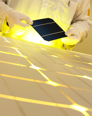
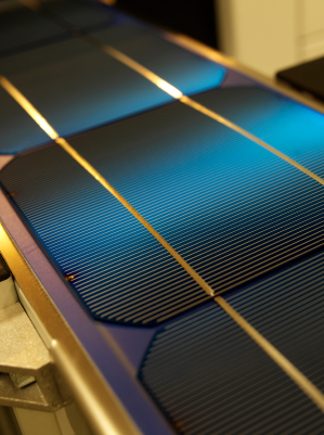
The Sicrys inks are high performance, state-of-the-art single crystal nano-metric conductive inks, based on PVN’s exclusive dispersion technology. They are made to offer a competitive edge to clients using inkjet printing for printed electronics and more. The Sicrys line of products is available in silver or copper-based form, ensuring maximum conductivity at a lowest cost.
How is this going to affect 3D printing? Through the development and modification of current inkjet 3D printing technologies – such as Stratasys Polyjet technology (and 3D System’s MultiJet Modeling) – It will become possible to directly 3D print electronic-capable products, such as photovoltaics, printed circuit boards, RFID, sensors, smart cards, touchscreens and advanced packaging.
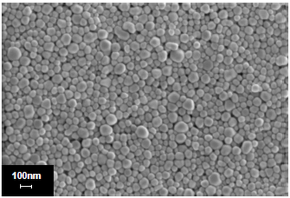
 “The idea here is to replace all the analogue production by using digital conductive printing, as part of an an additive process,” de la Vega explains. “We are primarily an ink company and we are developing inks that differ from anything else currently on the market. First of all, we have both silver and copper inks. Copper is safer and does not oxidize as easily. Our inks are made of nanometer particles; they are very special single crystal particles with enhanced properties that enable better electrical conductivity and stability. Our inks enable high throughput 24/7 printing for a highly industrialised process.”
Another aspect that, according to de la Vega, will help bring 3D printed electronics into the mainstream is that PVN’s inks are extremely low cost, with end prices that – even depending on quantity – are about one third of other nanometal particle conductive inks on the market. “We use a water-based process that is extremely cost effective,” he explains, “so much so that we can even compete with the prices of standard PolyJet resins in terms of pricing.”
To make end products, the inks can either be applied by ink jetting on pre-manufactured plastic parts, such as, for example, polycarbonate for mobile phone antennas, or they will be able to be 3D printed directly into the photopolymers during 3D printing. For this, the strategy by PVN is to focus exclusively on the inks and actively collaborate with hardware manufacturers to find the best compatibility with their own materials and processes. Recently, PVN signed a collaboration deal with a large PCB manufacturer in Israel and a consumer electronics company based in the USA and China.
 As recently as last November, PVN won the IDTechEx Award for Best Development in Materials for 3D Printing for its Sicrys materials and their potential in accelerating the adoption of solar photovoltaics (PV) and printed electronics (PE). “We are honored to receive this award from such an influential, high-profile organization, being recognized for the hard work that our team pours into developing our unique inks,” said Mr. de la Vega. “In order for the printed electronics industry to grow as anticipated, cost-efficient inks that enable mass production digital inkjet printing are necessary. We work with manufacturers of printed electronics including printed circuit boards, antennas and others to enable significant technological advancements.”
PVN has a production capacity of hundreds of kilograms and is specifically targeting the market for mass end-use products and parts. This might not mean we are going to see a fully 3D printed consumer electronic product – like a smartphone – in 2016, but this is the year when the foundations are going to be set in place for this to happen in the future.