

Researchers at Stanford University and Aalto University have built and tested a 3D printed panel that simultaneously handles six wireless signals across different frequencies, angles, and polarizations, boosting signal strength and channel capacity, with no active components of any kind.
The research was conducted by Mohammad M. Asgari, Shuai S. A. Yuan, and Viktar Asadchy at Aalto University’s Department of Electronics and Nanoengineering in Finland, in collaboration with Peter B. Catrysse, Haiwen Wang, and Shanhui Fan at Stanford University’s Ginzton Laboratory. The paper was published in Nature Communications on June 8, 2026.
What It Is and Why It’s Different
The device, called a metacrystal, is a block of patterned PLA plastic and air gaps designed to mount on walls or ceilings. It requires no power, no tunable components, and no control electronics. In testing, it boosted received signal strength by 20 to 24 dB in a non-line-of-sight scenario and improved channel capacity by up to 139% over the same environment without the panel.
The architecture differs from conventional intelligent reflecting surfaces, which are typically flat, single-layer structures optimized for one scenario, one frequency band, one polarization, one angle of arrival. Covering a real environment with multiple transmitters across different bands usually means multiple separate panels, or active electronics to switch between configurations.
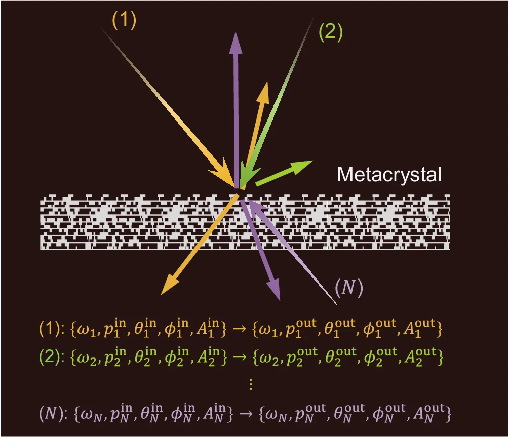
Metacrystals trade the flat form factor for physical depth. That thickness expands the number of structural parameters available during design, allowing a single geometry to encode independent responses to multiple incoming signals. An adjoint-based topology optimization algorithm takes a set of target behaviors, route this signal here, absorb that one, reflect another to a different angle, and generates the internal geometry needed to satisfy all of them at once. The result is a binary pattern of plastic and air that goes directly to a standard FDM printer.
What the Tests Showed
The paper presents three demonstrators. The first handled six simultaneous functionalities across three closely spaced frequencies (99, 100, and 102.53 GHz), two polarizations, and two angles of arrival, operating in both transmission and reflection at the same time. Simulated average efficiency across the six scenarios approached 99.99% under lossless material assumptions, though that figure applies to the idealized simulation, not fabricated hardware. For comparison, an equivalent single-layer metasurface design achieved no more than 2.28% average efficiency across the same six functionalities.
The second demonstrator targeted six independent reflective transformations for signals arriving at 0°, 20°, and 45° across both polarizations, reaching an average efficiency of 95.62% in simulation, with cross-talk into non-target channels remaining below 5% in most cases.
The third was the one actually built and measured. It handled four functionalities: polarization-insensitive anomalous reflection for normally incident signals, directed to an output angle of 72°, and near-complete absorption for signals arriving at 20°. Simulated absorption reached 90.47% and 96.34% for TE and TM polarizations respectively; measured anomalous reflection came in at 70.2% and 66.3%, below the simulated 84% and 78%, a gap the researchers attribute to fabrication tolerances and the small aperture of the prototype, which comprised only eight unit cells. A larger tiled version, assembled from four printed sections at 20.16 × 25.20 cm, delivered the 20–24 dB signal improvement and channel capacity gains of 8.2 Gbps (TE) and 14.3 Gbps (TM) in a non-line-of-sight scenario.
The consumables cost for the panel used in the communication link test came to around $15. Print time for the experimental sample was 34 hours, reducible to around 25 hours with a larger nozzle at some resolution trade-off.

Where It Falls Short
Bandwidth is the clearest constraint. The fabricated demonstrator achieved around 2% operational bandwidth for anomalous reflection, partly a design choice, since the third demonstrator was optimized for a single frequency. The first demonstrator showed that targeting multiple closely spaced frequencies during optimization can push this to 11% for TE polarization and 2.54% for TM, but systematic bandwidth engineering across both polarizations remains unsolved.
The number of simultaneous functions is also bounded by panel thickness and topology resolution. More functions require a thicker structure, and computational limits on the optimizer set a practical ceiling on complexity.
Real-world performance consistently fell short of simulation. Measured anomalous reflection efficiency came in around 10 percentage points below simulated values, traced to 3D printing tolerances and finite aperture effects. Both improve with larger panels, but the prototype tested only eight unit cells, a small sample by any standard. Extending the technology to sub-THz frequencies would require manufacturing precision beyond consumer FDM printers, and the passive architecture cannot adapt if transmitter or receiver positions shift significantly.
Fixed Environments, Smarter Panels
Reconfigurable intelligent surfaces, the dominant approach in 6G metasurface research, require tunable elements, bias electronics, and control circuitry that make large-area deployment too expensive for most buildings. The group’s bet is simpler: in factories, offices, and transit hubs, transmitters and receivers don’t move. A static panel that handles multiple signals at once, costs $15 in materials, and prints in under 25 hours makes the economic case on its own terms.
That logic has precedent. In 2023, researchers at the University of Sheffield developed 3D printed millimeter-wave antennas for 5G and 6G applications, demonstrating RF performance comparable to conventionally manufactured aerials at a fraction of the cost and production time.
More recently, a UC Berkeley, UCLA, and Lawrence Berkeley National Laboratory collaboration published work in June 2025 on ultralight 3D printed antennas operating at 19 GHz, inside the spectrum bands relevant to 6G, using a charge-programmed deposition method that cut antenna weight by 94%. Neither addressed the passive signal-routing and multifunctionality problem Stanford-Aalto University collaboration is targeting, but both established that 3D printing is a credible fabrication path for high-frequency electromagnetic structures, the same premise the metacrystal work builds on at higher complexity.
3D Printing Industry is inviting speakers for its 2026 Additive Manufacturing Applications (AMA) series, covering Energy, Healthcare, Automotive and Mobility, Aerospace, Space and Defense, and Software. Each online event focuses on real production deployments, qualification, and supply chain integration. Practitioners interested in contributing can complete the call for speakers form here.
To stay up to date with the latest 3D printing news, don’t forget to subscribe to the 3D Printing Industry newsletter or follow us on LinkedIn.
Explore the full Future of 3D Printing and Executive Survey series from 3D Printing Industry, featuring perspectives from CEOs, engineers, and industry leaders on the industrialization of additive manufacturing, 3D printing industry trends 2026, qualification, supply chains, and additive manufacturing industry analysis.
Featured image shows the concept of a multidimensional metacrystal. Image via Stanford University and Aalto University.